

| Distributor | Stock | Pricing | MOQ | PKG | Lead Time | Date Code | On Order Quantity | On Order Delivery | |
|---|---|---|---|---|---|---|---|---|---|
|
5,320 pcs
|
5320 pcs | On Request | 1 | On Request | On Request | 09+ | On Request | On Request |
| Category | |
| Manufacturer Name | |
| Configuration | |
| Current | |
| Drain to Source Voltage (Vdss) | |
| FET Feature | |
| Gate Charge (Qg) (Max) @ Vgs | |
| Input Capacitance (Ciss) (Max) @ Vds | |
| Mounting Type | |
| Operating Temperature | |
| Power | |
| Rds On (Max) @ Id, Vgs | |
| SVHC Present | |
| Storage Temperature | |
| Supplier Device Package | |
| Technology | |
| Vgs(th) (Max) @ Id |
The FDW2503N is a dual N-Channel MOSFET manufactured by On Semiconductor, utilizing advanced PowerTrench technology for low on-resistance and efficient power management. Rated for a drain-source voltage of 20V and continuous drain current of 5.5A, it features a maximum on-resistance of 21 mOhm at 4.5V Vgs and 35 mOhm at 2.5V Vgs.
The device is logic level gate compatible with a maximum gate threshold voltage of 1.5V at 250µA drain current. It exhibits low gate charge (17 nC max at 4.5V) and input capacitance (1082 pF max at 10V), facilitating fast switching with typical turn-on delay of 20 ns and turn-off delay of 38 ns.
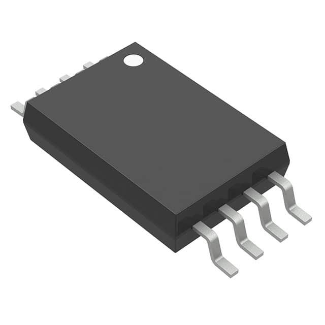
Housed in a low-profile 8-TSSOP package with surface mount mounting, the FDW2503N operates over a junction temperature range of -55°C to 150°C. Typical applications include load switching, motor drive, DC/DC conversion, and general power management in portable and battery-powered systems.
| Qty | Low | High |
|---|---|---|
| 433+ | $0.69 | $0.69 |
Estimated market price range - modelled values for guidance only, not live distributor offers.
The FDW2503N has a maximum drain-source voltage (Vdss) of 20 V.
The FDW2503N is available in an 8-TSSOP package (0.173", 4.40mm Width) with a supplier device package of 8-TSSOP.
The FDW2503N operates over a junction temperature range of -55°C to 150°C.
The FDW2503N is listed as RoHS3 Compliant, but this status is unverified.
The maximum on-resistance is 21 mOhm at Vgs = 4.5V and Id = 5.5A, and 35 mOhm at Vgs = 2.5V and Id = 4.2A.
The maximum gate threshold voltage is 1.5V at a drain current of 250 µA.
The maximum gate charge is 17 nC at Vgs = 4.5V and Vds = 10V, Id = 5.5A.