

| Distributor | Stock | Pricing | MOQ | PKG | Lead Time | Date Code | On Order Quantity | On Order Delivery | |
|---|---|---|---|---|---|---|---|---|---|
|
2 pcs
|
2 pcs | On Request | 1 | On Request | On Request | On Request | On Request | On Request |
| Category | |
| Manufacturer Name | |
| Configuration | |
| Continuous Drain-Source Diode Forward Current | |
| Current | |
| Diode Reverse Recovery Charge | |
| Diode Reverse Recovery Time | |
| Drain Current, Pulsed | |
| Drain Source On Resistance (Minimum/Typical @ VGS=2.5 V, ID=5 A) | |
| Drain Source On Resistance (Minimum/Typical @ VGS=4.5 V, ID=6 A, TJ=125 °C) | |
| Drain to Source Voltage (Vdss) | |
| FET Feature | |
| Forward Transconductance | |
| Gate Charge (Qg) (Max) @ Vgs | |
| Gate Resistance | |
| Gate-Drain Charge | |
| Gate-Source Charge | |
| Gate-Source Voltage | |
| Input Capacitance (Ciss) (Max) @ Vds | |
| Mounting Type | |
| On-State Drain Current | |
| Operating Temperature | |
| Output Capacitance | |
| Power | |
| Power Dissipation (Maximum @ TA = 25 °C, Note 1 b) | |
| Rds On (Max) @ Id, Vgs | |
| Reel Size | |
| Reverse Transfer Capacitance | |
| Standard Package Quantity | |
| Storage Temperature | |
| Supplier Device Package | |
| Tape & Reel | |
| Tape Width | |
| Technology | |
| Thermal Resistance, Junction-to-Ambient (Maximum @ Note 1 A) | |
| Thermal Resistance, Junction-to-Ambient (Maximum @ Note 1 b) | |
| Turn-Off Delay Time | |
| Turn-Off Fall Time | |
| Turn-On Delay Time | |
| Turn-On Rise Time | |
| Vgs(th) (Max) @ Id |
The FDW2501N is a dual N-channel 2.5V specified MOSFET built on Fairchild Semiconductor's advanced PowerTrench process, now part of onsemi. It is optimized for power management applications with a wide gate drive voltage range of 2.5V to 12V.
Key electrical specifications include a maximum drain-source voltage of 20V and a continuous drain current of 6A (at TA=25°C, Note 1a). The device offers low on-resistance: 18 mΩ typical at VGS=4.5V and 28 mΩ typical at VGS=2.5V. The logic level gate threshold voltage ranges from 0.4V minimum to 1.5V maximum, enabling direct drive from low-voltage logic.
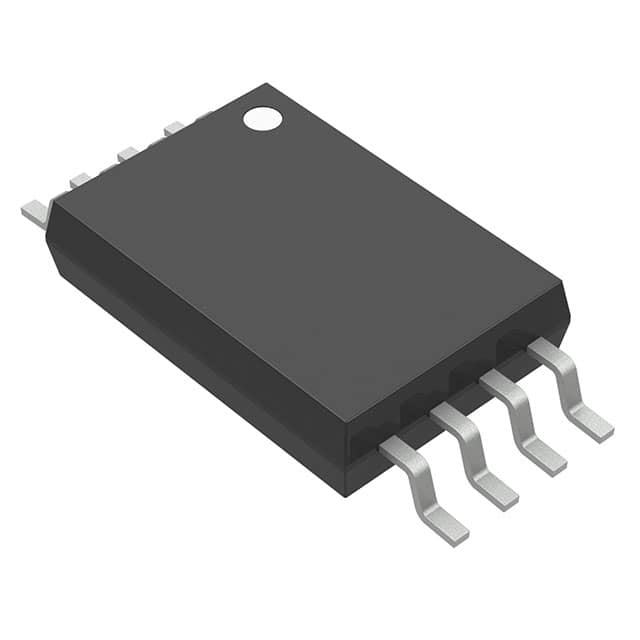
The FDW2501N is housed in a low-profile 8-TSSOP package (4.40mm width) suitable for surface mount assembly. It is supplied in tape and reel with 2500 units per reel (13" reel, 12mm tape width). Switching characteristics are suitable for moderate frequency applications, with typical turn-on delay of 10ns and fall time of 9.5ns.
Typical applications include load switches, motor drives, DC/DC conversion, and general power management in portable electronics. The device is rated for operating junction temperatures from -55°C to 150°C.
| Qty | Low | High |
|---|---|---|
| 209+ | $1.44 | $1.44 |
Estimated market price range - modelled values for guidance only, not live distributor offers.
The maximum drain-source voltage (Vdss) is 20 V.
The FDW2501N is housed in an 8-TSSOP package (0.173", 4.40mm Width) for surface mount assembly.
The operating junction temperature range is -55°C to 150°C.
The gate threshold voltage is 0.4 V minimum, 0.9 V typical, and 1.5 V maximum at VDS = VGS, ID = 250 µA.
The static drain-source on-resistance is 15.5 mΩ minimum and 18 mΩ typical at VGS = 4.5 V, ID = 6 A.
The FDW2501N is listed as RoHS3 compliant, but this status is unverified and should be confirmed with the manufacturer.
The moisture sensitivity level (MSL) is listed as 1 (unlimited), but this is unverified.