

| Category | |
| Manufacturer Name | |
| Current | |
| Drain to Source Voltage (Vdss) | |
| Drive Voltage (Max Rds On, Min Rds On) | |
| FET Type | |
| Gate Charge (Qg) (Max) @ Vgs | |
| Input Capacitance (Ciss) (Max) @ Vds | |
| Mounting Type | |
| Operating Temperature | |
| Power Dissipation (Max) | |
| Rds On (Max) @ Id, Vgs | |
| Supplier Device Package | |
| Technology | |
| Vgs (Max) | |
| Vgs(th) (Max) @ Id |
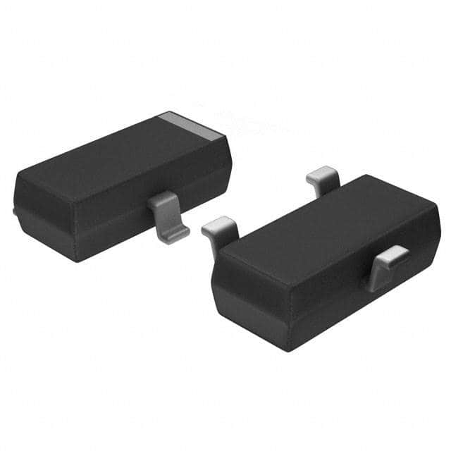
The FDV302P is a P-Channel enhancement-mode MOSFET manufactured by ON Semiconductor. It features a maximum drain-source voltage of 25V and a continuous drain current of 120mA at ambient temperature. The device uses MOSFET (Metal Oxide) technology.
Key electrical characteristics include a maximum on-resistance of 10 Ohms at 200mA and 4.5V gate drive, a gate threshold voltage of 1.5V at 250µA, and a maximum gate-source voltage of -8V. Input capacitance is 11pF at 10V, and gate charge is 0.31nC at 4.5V. Maximum power dissipation is 350mW at ambient temperature.
The FDV302P is designed for surface mount assembly and is available in TO-236-3, SC-59, and SOT-23-3 packages, with the supplier device package being SOT-23-3. It operates over a junction temperature range of -55°C to 150°C. This device is suitable for low-power switching and load management applications.
| Qty | Low | High |
|---|---|---|
| 3,000+ | $0.52 | $0.52 |
Estimated market price range - modelled values for guidance only, not live distributor offers.
25V.
TO-236-3, SC-59, SOT-23-3; supplier device package is SOT-23-3.
-55°C to 150°C (junction).
RoHS3 Compliant (unverified).
1.5V at 250µA.
10 Ohms maximum at 200mA and 4.5V gate drive.
350mW at ambient temperature.