

| Distributor | Stock | Pricing | MOQ | PKG | Lead Time | Date Code | On Order Quantity | On Order Delivery | |
|---|---|---|---|---|---|---|---|---|---|
|
5,924 pcs
|
5924 pcs | On Request | 1 | On Request | On Request | 09+ | On Request | On Request |
| Category | |
| Manufacturer Name | |
| Current | |
| Drain to Source Voltage (Vdss) | |
| Drive Voltage (Max Rds On, Min Rds On) | |
| FET Type | |
| Gate Charge (Qg) (Max) @ Vgs | |
| Input Capacitance (Ciss) (Max) @ Vds | |
| Mounting Type | |
| Operating Temperature | |
| Power Dissipation (Max) | |
| Rds On (Max) @ Id, Vgs | |
| Supplier Device Package | |
| Technology | |
| Vgs (Max) | |
| Vgs(th) (Max) @ Id |
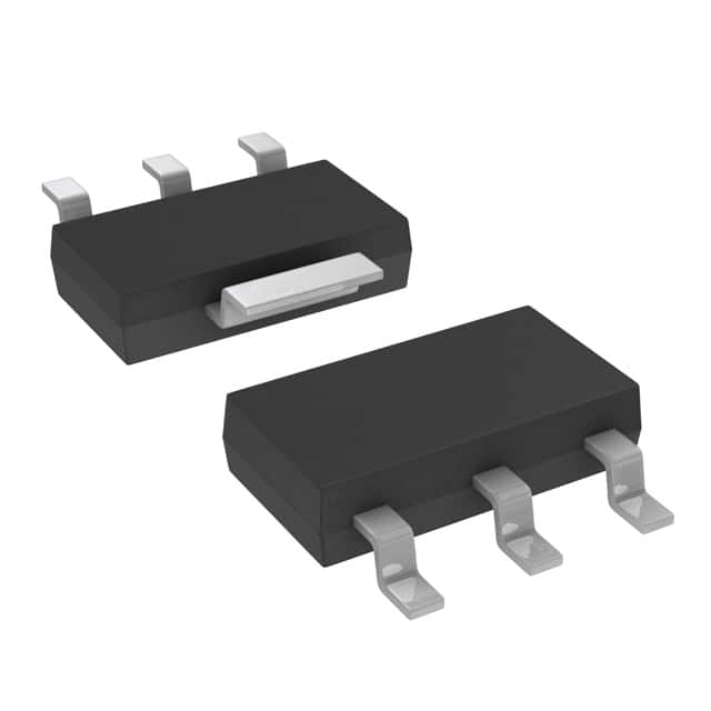
The FDT55AN06LA0 is an N-Channel PowerTrench MOSFET from ON Semiconductor, designed for efficient power switching in a compact SOT-223 surface-mount package. It is rated for a maximum drain-source voltage of 60V and a continuous drain current of 12.1A at 25°C with 10V gate drive. The device features a typical on-resistance of 36 mΩ (46 mΩ max) at VGS=10V and ID=11A, and 44 mΩ (55 mΩ max) at VGS=5V, enabling low conduction losses.
Key electrical characteristics include a gate threshold voltage range of 1V to 3V, total gate charge of 7.6 nC typical (10 nC max), and input capacitance of 849 pF typical (1130 pF max). Switching times are fast with typical turn-on delay of 10 ns and rise time of 24 ns. The device also offers avalanche energy capability of 34 mJ and a body diode with low reverse recovery charge.
The MOSFET is suitable for applications such as motor/body load control, power train management, DC-AC converters, and distributed power architectures. It operates over a junction temperature range of -55°C to +150°C and is RoHS compliant.
The maximum drain-source voltage (Vdss) is 60V.
The FDT55AN06LA0 is available in a SOT-223 surface mount package.
The operating junction temperature range is -55°C to +150°C.
Yes, the FDT55AN06LA0 is RoHS compliant as stated in the datasheet.
The gate threshold voltage (Vgs(th)) is typically 1V minimum and 3V maximum at ID=250µA.
The maximum on-resistance (Rds(on)) at VGS=10V and ID=11A is 46 mΩ.
The typical total gate charge (Qg) is 7.6 nC at VDS=30V, ID=11A, VGS=0V to 5V.