

Have a small number of parts or want to add parts manually? Request Quote manually

Search across all market segments

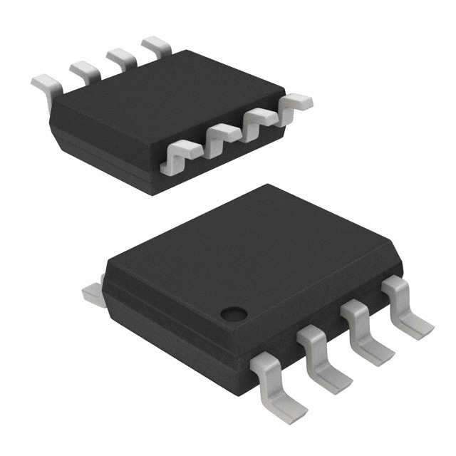
FDS8978 Dual N-channel MOSFET with 30V drain-source voltage, 7.5A continuous drain current, and 18mΩ on-resistance at 10V gate drive. Supplied in 8-SOIC surface mount package.
Mfr Part #:

FDS8978

Available from 2 distributors
Mfr Name: On Semiconductor
On Semiconductor
Dual N-channel MOSFET with 30V drain-source voltage, 7.5A continuous drain current, and 18mΩ on-resistance at 10V gate drive. Supplied in 8-SOIC surface mount package.
Total Stock: 1,839 pcs
$ Price Range: $0.15 - $0.76

FDS8978 Available from 2 distributors

Authorised
Non-Authorised
Distributor Stock Pricing MOQ PKG Lead Time Date Code On Order Quantity On Order Delivery
Non-Authorised Inventory information
1,643 pcs
1643 pcs On Request 1 On Request On Request On Request On Request On Request
Non-Authorised Inventory information
196 pcs
196 pcs On Request 1 On Request On Request 15+ On Request On Request

FDS8978 Specifications Quick View

Most important parameters for selection – full specs in datasheet.
Category
Manufacturer Name
Configuration
Current
Drain Current Continuous (Maximum @ Vgs=4.5 V, Tc=25 °C)
Drain Current, Pulsed
Drain to Source Voltage (Vdss)
Drain-Source Breakdown Voltage
Drain-Source On Resistance (Typical/Maximum @ I_D=6.9 A, V_GS=4.5 V)
Drain-Source On Resistance (Typical/Maximum @ I_D=7.5 A, V_GS=10 V)
Drain-Source On Resistance (Typical/Maximum @ I_D=7.5 A, V_GS=10 V, T_C=150 °C)
FET Feature
Gate Charge (Qg) (Max) @ Vgs
Gate Resistance (Typical/Maximum @ V_GS=0.5 V, f=1 MHz)
Gate Threshold Voltage (Minimum/Maximum @ I_D=250 µA, V_DS=V_GS)
Gate-Source Voltage (Maximum)
Gate-to-Source Leakage Current
Input Capacitance (Ciss) (Max) @ Vds
Input Capacitance (Typical/Maximum @ V_DS=15 V, V_GS=0 V, f=1 MHz)
Mounting Type
Operating Temperature
Output Capacitance (Typical)
Power
Power Dissipation Derating Factor
Rds On (Max) @ Id, Vgs
Reverse Transfer Capacitance (Typical)
Single Pulse Avalanche Energy
Storage Temperature Range
Supplier Device Package
Technology
Thermal Resistance - Junction to Case
Thermal Resistance, Junction to Ambient (Nominal @ 0.02 in² pad of 2 oz copper)
Thermal Resistance, Junction to Ambient (Nominal @ 0.5 in² pad of 2 oz copper)
Thermal Resistance, Junction to Ambient (Nominal @ minimum pad)
Vgs(th) (Max) @ Id
Zero Gate Voltage Drain Current (Maximum @ V_DS=24 V, V_GS=0 V, T_J=150 °C)
Zero Gate Voltage Drain Current (Maximum @ V_DS=24 V, V_GS=0 V, T_J=25 °C)

FDS8978 Description

Short technical summary and product information.

The FDS8978 is a dual N-channel enhancement mode MOSFET designed for efficient power management in DC/DC converters. It features two independent MOSFETs in a single 8-SOIC package, offering a space-saving solution for synchronous rectification and switching applications.


Key electrical specifications include a maximum drain-source voltage of 30V and continuous drain current of 7.5A at 10V gate drive (6.9A at 4.5V). The on-resistance is typically 14mΩ and maximum 18mΩ at 10V gate bias, with a maximum of 21mΩ at 4.5V. The device supports logic level gate drive, allowing direct interface with low-voltage controllers.


The MOSFET incorporates trench technology for low gate charge (26nC typical) and fast switching. Gate threshold voltage ranges from 1.2V to 2.5V. Thermal characteristics include junction-to-case resistance of 40°C/W and junction-to-ambient of 78°C/W (on 0.5 in² copper pad).


Packaged in an 8-SOIC (0.154", 3.90mm width) surface mount package, the FDS8978 is RoHS3 compliant with MSL 1 (unlimited) moisture sensitivity. It is suitable for battery management, load switching, and power supply designs.

FDS8978 Quick Information

Product Type: MOSFET
Canonical Name: Dual N-Channel MOSFET 30V 7.5A 8-SOIC
Subcategory: Dual N-Channel MOSFET

FDS8978 Compliance

RoHS Status: RoHS Compliant
Moisture Sensitivity Level (MSL): 1 Unlimited
REACH Status: REACH Unaffected

FDS8978 Estimated Pricing

Qty Low High
1+ $0.76 $0.76
10+ $0.47 $0.47
50+ $0.35 $0.35
100+ $0.30 $0.30
500+ $0.23 $0.23
3,000+ $0.18 $0.18
9,000+ $0.15 $0.15

Estimated market price range - modelled values for guidance only, not live distributor offers.

FDS8978 Features

  • Dual N-channel MOSFET in 8-SOIC package.
  • Low on-resistance: 18mΩ max at 10V gate.
  • Logic level gate drive for low-voltage control.
  • Low gate charge: 26nC max for fast switching.
  • High pulsed drain current: 49A maximum.

FDS8978 Applications

  • Synchronous rectification in DC/DC converters.
  • Load switching in portable electronics.
  • Battery management and protection circuits.
  • Power supply output stage switching.

FDS8978 FAQs

7 frequently asked questions generated from this part’s specifications.
What is the maximum drain-source voltage of the FDS8978?

30 V.

What is the continuous drain current rating?

7.5 A at Vgs=10V, Tc=25°C; 6.9 A at Vgs=4.5V, Tc=25°C.

What is the on-resistance of this MOSFET?

Maximum 18 mΩ at Vgs=10V, Id=7.5A; maximum 21 mΩ at Vgs=4.5V, Id=6.9A.

What package does the FDS8978 come in?

8-SOIC (0.154", 3.90mm Width) surface mount package.

What is the operating temperature range?

-55°C to 150°C (junction temperature).

Is the FDS8978 RoHS compliant?

Yes, RoHS3 compliant according to existing database records (not verified with document).

What is the gate threshold voltage range?

Minimum 1.2V, maximum 2.5V at Id=250µA.

Home
Categories
Submit RFQ
Login
Account

Categories