

| Distributor | Stock | Pricing | MOQ | PKG | Lead Time | Date Code | On Order Quantity | On Order Delivery | |
|---|---|---|---|---|---|---|---|---|---|
|
1,236 pcs
|
1236 pcs | On Request | 1 | On Request | On Request | On Request | On Request | On Request |
| Category | |
| Manufacturer Name | |
| Current | |
| Drain to Source Voltage (Vdss) | |
| Drive Voltage (Max Rds On, Min Rds On) | |
| FET Type | |
| Gate Charge (Qg) (Max) @ Vgs | |
| Halogen Free | |
| Input Capacitance (Ciss) (Max) @ Vds | |
| Mounting Type | |
| Operating Temperature | |
| Power Dissipation (Max) | |
| Rds On (Max) @ Id, Vgs | |
| Supplier Device Package | |
| Tape & Reel | |
| Technology | |
| Vgs (Max) | |
| Vgs(th) (Max) @ Id |
The FDS86267P is a P-Channel MOSFET manufactured by onsemi using the advanced POWERTRENCH process with shielded gate technology. This process is optimized for low on-state resistance while maintaining superior switching performance. The device is rated for a maximum drain-source voltage of -150V and a continuous drain current of -2.2A at 25°C ambient temperature.
The MOSFET features a maximum drain-source on-resistance of 255mΩ at VGS=-10V and ID=-2.2A, and 290mΩ at VGS=-6V and ID=-2A. The gate threshold voltage ranges from -2V minimum to -4V maximum with a typical value of -3V. The device supports a gate-source voltage of ±25V and has a maximum gate charge of 16nC at VGS=-10V.
This product is optimized for fast switching applications as well as load switch applications. It is suitable for use as an active clamp switch or load switch. The device is 100% UIL tested and features a single pulse avalanche energy rating of 54mJ. Input capacitance is 1130pF at VDS=-75V.
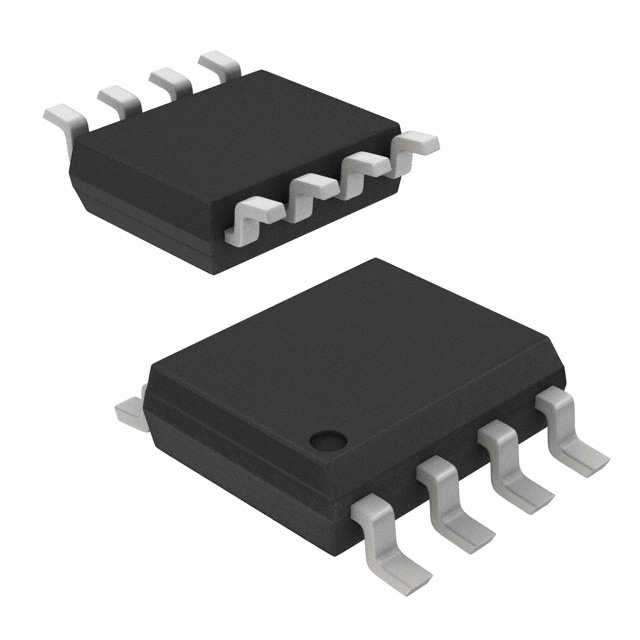
The FDS86267P is available in an 8-SOIC surface-mount package (0.154", 3.90mm width) and is supplied in tape and reel packaging with a standard quantity of 2500 pieces. The device operates over a junction temperature range of -55°C to 150°C with power dissipation ratings of 2.5W (Note 1a) and 1W (Note 1b) at 25°C ambient.
| Qty | Low | High |
|---|---|---|
| 1+ | $2.60 | $2.60 |
| 10+ | $1.67 | $1.67 |
| 100+ | $1.13 | $1.13 |
| 500+ | $0.96 | $0.96 |
| 2,500+ | $0.96 | $0.96 |
Estimated market price range - modelled values for guidance only, not live distributor offers.
The maximum drain-source voltage (VDS) is -150V.
The maximum continuous drain current is -2.2A at Ta=25°C. The pulsed drain current rating is -34A.
The maximum drain-source on-resistance is 255mΩ at VGS=-10V and ID=-2.2A, and 290mΩ at VGS=-6V and ID=-2A.
The operating junction temperature range is -55°C to 150°C.
The FDS86267P is available in an 8-SOIC surface-mount package (0.154", 3.90mm width), also known as SOIC8.
Yes, the FDS86267P is RoHS3 compliant, Pb-free, and halide free as verified from the datasheet.
The gate threshold voltage ranges from -2V minimum to -4V maximum, with a typical value of -3V at ID=-250µA.