

| Distributor | Stock | Pricing | MOQ | PKG | Lead Time | Date Code | On Order Quantity | On Order Delivery | |
|---|---|---|---|---|---|---|---|---|---|
|
1,540 pcs
|
1540 pcs | On Request | 1 | On Request | On Request | 12+ | On Request | On Request | |
|
970 pcs
|
970 pcs | On Request | 1 | On Request | On Request | N/A | On Request | On Request | |
|
15 pcs
|
15 pcs | On Request | 1 | On Request | On Request | On Request | On Request | On Request |
| Category | |
| Manufacturer Name | |
| Configuration | |
| Current | |
| Drain Current (Continuous) (Maximum @ Q 2) | |
| Drain Current (Pulsed) (Maximum @ Q 1) | |
| Drain Current (Pulsed) (Maximum @ Q 2) | |
| Drain to Source Voltage (Vdss) | |
| FET Feature | |
| Gate Charge (Qg) (Max) @ Vgs | |
| Gate Charge (Qg) (Typical @ Q 1, Vgs=10 V) | |
| Gate Resistance Tested | |
| Gate-Source Voltage (Vgss) | |
| Input Capacitance (Ciss) (Max) @ Vds | |
| Mounting Type | |
| Operating Temperature | |
| Power | |
| Power Dissipation (Maximum @ Dual operation) | |
| Power Dissipation (Maximum @ Single operation (Note 1 A) | |
| Power Dissipation (Maximum @ Single operation, Note 1 c) | |
| Rds On (Max) @ Id, Vgs | |
| Rds(on) (Maximum @ Q 1, Vgs=4.5 V) | |
| Rds(on) (Maximum @ Q 2, Vgs=10 V) | |
| Rds(on) (Maximum @ Q 2, Vgs=4.5 V) | |
| Standard Package Quantity | |
| Supplier Device Package | |
| Tape & Reel | |
| Technology | |
| Thermal Resistance Junction to Ambient (RθJA) | |
| Thermal Resistance Junction-to-Case (RθJC) | |
| Vgs(th) (Max) @ Id |
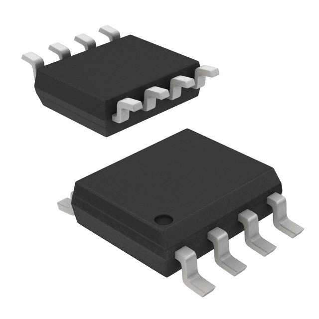
The FDS6900AS is a dual N-channel MOSFET from On Semiconductor, integrating two 30V logic level MOSFETs in a compact 8-SOIC package. The high-side MOSFET (Q1) is optimized for low switching losses with a typical gate charge of 11 nC, while the low-side MOSFET (Q2) is optimized for low conduction losses with a maximum Rds(on) of 22 mOhm at Vgs=10V. Q2 also includes an integrated SyncFET Schottky diode for improved efficiency.
Key electrical specifications include a drain-source voltage rating of 30V, continuous drain current of 6.9A for Q1 and 8.2A for Q2, and pulsed drain current up to 20A and 30A respectively. The device is rated for a junction temperature range of -55°C to 150°C and has a maximum power dissipation of 2W for dual operation. Thermal resistance is 78°C/W junction-to-ambient and 40°C/W junction-to-case.
This MOSFET array is designed for synchronous DC-DC power supplies, particularly in notebook computers and other battery-powered electronics. The logic-level gate threshold (3V max at 250µA) allows direct drive from low-voltage controllers. The package is surface-mount 8-SOIC, supplied in tape and reel packaging with 2500 pieces per reel.
| Qty | Low | High |
|---|---|---|
| 362+ | $0.83 | $0.83 |
Estimated market price range - modelled values for guidance only, not live distributor offers.
The maximum drain-source voltage (Vdss) is 30 V for both MOSFETs.
Q1 continuous drain current is 6.9 A, Q2 is 8.2 A.
The maximum Rds(on) of Q2 at Vgs=10V is 22 mOhm.
The junction temperature range is -55°C to 150°C.
The device is packaged in an 8-SOIC (0.154", 3.90mm Width) surface mount package.
Yes, the device is RoHS3 compliant and Pb-Free as per the datasheet.
The typical gate charge (Qg) of Q1 at Vgs=10V is 11 nC.