

| Distributor | Stock | Pricing | MOQ | PKG | Lead Time | Date Code | On Order Quantity | On Order Delivery | |
|---|---|---|---|---|---|---|---|---|---|
|
120,533 pcs
|
120533 pcs | On Request | 1 | On Request | On Request | On Request | On Request | On Request | |
|
20,000 pcs
|
20000 pcs | On Request | 1 | On Request | On Request | On Request | On Request | On Request | |
|
6,413 pcs
|
6413 pcs | On Request | 1 | On Request | On Request | On Request | On Request | On Request | |
|
6,000 pcs
|
6000 pcs | On Request | 1 | On Request | On Request | On Request | On Request | On Request | |
|
2,000 pcs
|
2000 pcs | On Request | 1 | On Request | On Request | On Request | On Request | On Request | |
|
1,964 pcs
|
1964 pcs | On Request | 1 | On Request | On Request | 903 | On Request | On Request | |
|
1,283 pcs
|
1283 pcs | On Request | 1 | On Request | On Request | 1441 | On Request | On Request | |
|
1,000 pcs
|
1000 pcs | On Request | 1 | On Request | On Request | On Request | On Request | On Request | |
|
1,000 pcs
|
1000 pcs | On Request | 1 | On Request | On Request | On Request | On Request | On Request |
| Category | |
| Manufacturer Name | |
| Configuration | |
| Current | |
| Drain to Source Voltage (Vdss) | |
| FET Feature | |
| Gate Charge (Qg) (Max) @ Vgs | |
| Input Capacitance (Ciss) (Max) @ Vds | |
| Mounting Type | |
| Operating Temperature | |
| Power | |
| Rds On (Max) @ Id, Vgs | |
| Supplier Device Package | |
| Tape & Reel | |
| Technology | |
| Vgs(th) (Max) @ Id |
The FDS6898A is a dual N-channel logic level PowerTrench MOSFET from On Semiconductor, designed for low voltage and battery powered applications. It supports a maximum drain-source voltage of 20 V and a continuous drain current of 9.4 A, with pulsed current capability up to 38 A.
The device features a low on-resistance of 14 mΩ typical at VGS = 4.5 V and 18 mΩ typical at VGS = 2.5 V, enabling efficient switching with reduced conduction losses. The logic level gate allows direct drive from low voltage control signals. Total gate charge is 16 nC typical, supporting fast switching performance in PWM applications.
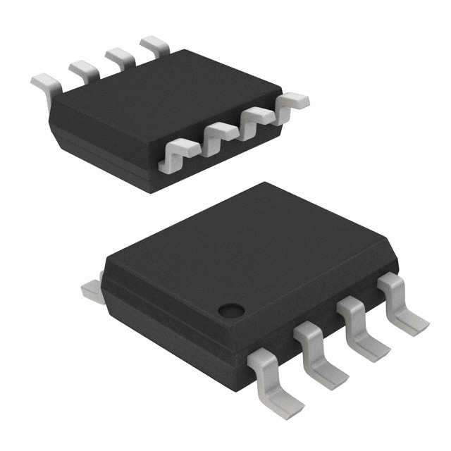
Housed in an 8-SOIC package, the FDS6898A operates over a junction temperature range of -55°C to +150°C. The dual MOSFET configuration is suitable for synchronous rectification, load switching, and dc-dc converter output stages where space is limited.
| Qty | Low | High |
|---|---|---|
| 1+ | $1.84 | $1.84 |
| 10+ | $1.16 | $1.16 |
| 100+ | $0.76 | $0.76 |
| 500+ | $0.61 | $0.61 |
| 2,500+ | $0.61 | $0.61 |
| 5,000+ | $0.59 | $0.59 |
| 10,000+ | $0.47 | $0.47 |
| 25,000+ | $0.47 | $0.47 |
Estimated market price range - modelled values for guidance only, not live distributor offers.
The FDS6898A has a maximum drain-source voltage of 20 V.
The continuous drain current is 9.4 A, with pulsed current capability up to 38 A.
Rds(on) is 14 mΩ max at VGS=4.5V and 18 mΩ max at VGS=2.5V.
The FDS6898A is available in an 8-SOIC (0.154" width, 3.90mm) surface mount package.
The operating junction temperature range is -55°C to +150°C.
Listed as RoHS3 compliant per existing database records; not verified from datasheet.
Total gate charge is 16 nC typical and 23 nC maximum at VGS=4.5V.