

Have a small number of parts or want to add parts manually? Request Quote manually

Search across all market segments

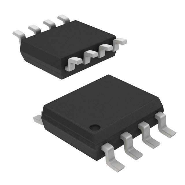
FDS6572A The FDS6572A is a 20V N-Channel PowerTrench MOSFET in an 8-SOIC package. It supports 16A continuous drain current with a low 6mΩ maximum on-resistance at 4.5V gate drive.
Mfr Part #:

FDS6572A

Available from 1 distributors
Mfr Name: On Semiconductor
On Semiconductor
The FDS6572A is a 20V N-Channel PowerTrench MOSFET in an 8-SOIC package. It supports 16A continuous drain current with a low 6mΩ maximum on-resistance at 4.5V gate drive.
Total Stock: 2,289 pcs
$ Price Range: $2.11

FDS6572A Available from 1 distributor

Authorised
Non-Authorised
Distributor Stock Pricing MOQ PKG Lead Time Date Code On Order Quantity On Order Delivery
Non-Authorised Inventory information
2,289 pcs
2289 pcs On Request 1 On Request On Request 1105+ On Request On Request

FDS6572A Specifications Quick View

Most important parameters for selection – full specs in datasheet.
Category
Manufacturer Name
Current
Drain Current, Pulsed
Drain to Source Voltage (Vdss)
Drain-Source Breakdown Voltage
Drive Voltage (Max Rds On, Min Rds On)
FET Type
Fall Time (Typical/Maximum @ Vdd=-10 V, Id=-1 A, Vgs=-4.5 V, Rgen=6Ω)
Forward Transconductance (Typ)
Gate Charge (Qg) (Max) @ Vgs
Gate-Drain Charge (Typ)
Gate-Source Charge (Typ)
Halogen Free
Input Capacitance (Ciss) (Max) @ Vds
Maximum Continuous Drain-Source Diode Forward Current
Mounting Type
Operating Temperature
Output Capacitance (Coss) (Typ) @ Vds
Power Dissipation (Max)
Rds On (Max) @ Id, Vgs
Reel Size
Reverse Transfer Capacitance (Crss) (Typ) @ Vds
Rise Time (Typical/Maximum @ Vdd=-10 V, Id=-1 A, Vgs=-4.5 V, Rgen=6Ω)
SVHC Present
Supplier Device Package
Tape & Reel Quantity
Tape Width
Technology
Thermal Resistance - Junction to Case
Thermal Resistance, Junction-to-Ambient (Note 1a)
Turn-Off Delay Time (Typical/Maximum @ Vdd=-10 V, Id=-1 A, Vgs=-4.5 V, Rgen=6Ω)
Turn-On Delay Time (Typical/Maximum @ Vdd=-10 V, Id=-1 A, Vgs=-4.5 V, Rgen=6Ω)
Vgs (Max)
Vgs(th) (Max) @ Id
Zero Gate Voltage Drain Current
diode_forward_voltage (Typical/Maximum @ Is=2.1 A, Vgs=0 V)
drain_source_on_resistance (Typical/Maximum @ Id=14 A, Vgs=2.5 V)
drain_source_on_resistance (Typical/Maximum @ Id=16 A, Vgs=4.5 V)
drain_source_on_resistance (Typical/Maximum @ Id=16 A, Vgs=4.5 V, Tj=125 °C)
gate_body_leakage (Maximum @ VGS=±12 V, VDS=0 V)
gate_threshold_voltage (Minimum/Typical/Maximum @ ID = 250 µA)
power_dissipation (Maximum @ TA = 25 °C, Note 1 b)
power_dissipation (Maximum @ Ta = 25 °C (Note 1 c)
total_gate_charge (Typical/Maximum @ Vds=10 V, Id=16 A, Vgs=4.5 V)

FDS6572A Description

Short technical summary and product information.

The FDS6572A is an N-Channel PowerTrench MOSFET designed for DC/DC converter applications using synchronous or conventional switching PWM controllers. It is rated for a maximum drain-to-source voltage of 20V and a continuous drain current of 16A at 25°C ambient temperature, with a pulsed drain current rating of 80A.


The device features a maximum on-resistance of 6mΩ at VGS=4.5V and 8mΩ at VGS=2.5V, enabling efficient low-voltage switching. Total gate charge is 57nC typical, and input capacitance is 5914pF at VDS=10V. The MOSFET is optimized for low gate charge, low RDS(ON), and fast switching speed.


The FDS6572A is available in an 8-SOIC surface-mount package with a junction-to-ambient thermal resistance of 50°C/W and a maximum power dissipation of 2.5W at 25°C ambient. It operates over a junction temperature range of -55°C to 175°C. The device is supplied in 13-inch tape and reel packaging with 2500 units per reel.

FDS6572A Quick Information

Product Type: N-Channel MOSFET
Canonical Name: 20V N-Channel PowerTrench MOSFET
Subcategory: Single N-Channel MOSFET

FDS6572A Compliance

RoHS Status: RoHS Compliant
Moisture Sensitivity Level (MSL): 1 Unlimited
REACH Status: REACH Unaffected
Lead Free: Yes

FDS6572A Estimated Pricing

Qty Low High
142+ $2.11 $2.11

Estimated market price range - modelled values for guidance only, not live distributor offers.

FDS6572A Features

  • 20V drain-source voltage rating.
  • 16A continuous drain current capability.
  • 6mΩ maximum on-resistance at 4.5V.
  • Low 57nC typical gate charge.
  • Surface mount 8-SOIC package.

FDS6572A Applications

  • Used in DC/DC converter circuits.
  • Suitable for synchronous PWM controllers.
  • Ideal for low-voltage power switching.
  • Works in conventional switching converters.

FDS6572A FAQs

7 frequently asked questions generated from this part’s specifications.
What is the maximum drain-to-source voltage of the FDS6572A?

The maximum drain-to-source voltage (VDSS) is 20V.

What is the maximum continuous drain current of the FDS6572A?

The maximum continuous drain current is 16A at 25°C ambient temperature.

What is the on-resistance of the FDS6572A?

The maximum on-resistance is 6mΩ at VGS=4.5V and 8mΩ at VGS=2.5V.

What package is the FDS6572A available in?

The FDS6572A is available in an 8-SOIC surface mount package.

What is the operating temperature range of the FDS6572A?

The operating junction temperature range is -55°C to 175°C.

What is the gate threshold voltage of the FDS6572A?

The gate threshold voltage ranges from 0.6V minimum to 1.5V maximum, with a typical value of 0.8V at ID=250µA.

What is the total gate charge of the FDS6572A?

The total gate charge is 57nC typical and 80nC maximum at VDS=10V, ID=16A, VGS=4.5V.

Home
Categories
Submit RFQ
Login
Account

Categories