

| Distributor | Stock | Pricing | MOQ | PKG | Lead Time | Date Code | On Order Quantity | On Order Delivery | |
|---|---|---|---|---|---|---|---|---|---|
|
100 pcs
|
100 pcs | On Request | 1 | On Request | On Request | 0636+ | On Request | On Request |
| Category | |
| Manufacturer Name | |
| Configuration | |
| Current | |
| Drain Current (Continuous) (Maximum @ Q 2 (P-Channel) @ TA=+25 °C) | |
| Drain Current (Pulsed) (Q1 (N-Channel) and Q2 (P-Channel)) | |
| Drain to Source Voltage (Vdss) | |
| Gate Charge (Qg) (Max) @ Vgs | |
| Gate Resistance (Typical @ Q 1 (N-Channel), f=1 MHz) | |
| Gate Resistance (Typical @ Q 2 (P-Channel), f=1 MHz) | |
| Gate Threshold Voltage (Minimum/Typical/Maximum @ Q 2 (P-Channel), Vds=Vgs, Id=-250 µA) | |
| Gate-Source Voltage (Q1 (N-Channel) and Q2 (P-Channel)) | |
| Input Capacitance (Ciss) (Max) @ Vds | |
| Input Capacitance (Typical @ Q 2 (P-Channel), Vds=-20 V, Vgs=0 V, f=1 MHz) | |
| Lead Spacing | |
| Lead Style | |
| Mounting Type | |
| On-Resistance (Typical/Maximum @ Q 1 (N-Channel), Vgs=10 V, Id=5.5 A, Tj=125 °C) | |
| On-Resistance (Typical/Maximum @ Q 1 (N-Channel), Vgs=7 V, Id=4.8 A) | |
| On-Resistance (Typical/Maximum @ Q 2 (P-Channel), Vgs=-10 V, Id=-4.4 A) | |
| On-Resistance (Typical/Maximum @ Q 2 (P-Channel), Vgs=-10 V, Id=-4.4 A, Tj=125 °C) | |
| On-Resistance (Typical/Maximum @ Q 2 (P-Channel), Vgs=-4.5 V, Id=-3.8 A) | |
| Operating Temperature | |
| Output Capacitance (Typical @ Q 1 (N-Channel), Vds=20 V, Vgs=0 V, f=1 MHz) | |
| Output Capacitance (Typical @ Q 2 (P-Channel), Vds=-20 V, Vgs=0 V, f=1 MHz) | |
| Power | |
| Power Dissipation (Maximum @ Dual operation) | |
| Rds On (Max) @ Id, Vgs | |
| Reel Size | |
| Reverse Transfer Capacitance (Typical @ Q 1 (N-Channel), Vds=20 V, Vgs=0 V, f=1 MHz) | |
| Reverse Transfer Capacitance (Typical @ Q 2 (P-Channel), Vds=-20 V, Vgs=0 V, f=1 MHz) | |
| Standard Package Quantity | |
| Storage Temperature | |
| Supplier Device Package | |
| Tape & Reel | |
| Tape Width | |
| Technology | |
| Thermal Resistance, Junction-to-Ambient (Note 1a) | |
| Thermal Resistance, Junction-to-Case (Note 1) | |
| Vgs(th) (Max) @ Id |
The FDS4895C is a dual N and P-Channel enhancement mode power MOSFET produced using Fairchild Semiconductor's advanced PowerTrench process, optimized for low on-state resistance and superior switching performance. The N-channel MOSFET (Q1) is rated for 40V drain-source voltage with a continuous drain current of 5.5A at 25°C, while the P-channel (Q2) is rated for -40V with -4.4A continuous current. Both channels can handle pulsed currents up to 20A.
On-resistance is typically 32mΩ for the N-channel at Vgs=10V (max 39mΩ) and 37mΩ for the P-channel at Vgs=-10V (max 46mΩ). Gate threshold voltages are 2V-5V for N-channel and -1V to -3V for P-channel. Input capacitance is 410pF (N) and 1050pF (P), with total gate charge of 10nC for the N-channel. The device is designed for applications such as motor control and DC/DC conversion.
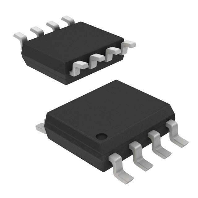
Packaged in an 8-SOIC (0.154", 3.90mm Width) surface mount package, the FDS4895C offers a maximum power dissipation of 900mW for single operation on a standard FR-4 board with 1 in² copper pad, and 2W for dual operation. Junction temperature range is -55°C to 150°C. Thermal resistance is 78°C/W junction-to-ambient (note 1a) and 40°C/W junction-to-case.
| Qty | Low | High |
|---|---|---|
| 505+ | $0.59 | $0.59 |
Estimated market price range - modelled values for guidance only, not live distributor offers.
The maximum drain-source voltage is 40V for both N and P-channel MOSFETs.
It is available in an 8-SOIC (0.154", 3.90mm Width) surface mount package.
The operating junction temperature range is -55°C to 150°C.
The RoHS status is listed as RoHS3 Compliant, but this is unverified and should be confirmed with the manufacturer.
The typical on-resistance is 32mΩ at Vgs=10V, Id=5.5A, with a maximum of 39mΩ.
The continuous drain current is -4.4A at 25°C ambient.
The gate threshold voltage range is 2V min, 3.7V typ, 5V max at Id=250µA.