

| Distributor | Stock | Pricing | MOQ | PKG | Lead Time | Date Code | On Order Quantity | On Order Delivery | |
|---|---|---|---|---|---|---|---|---|---|
|
5,245 pcs
|
5245 pcs | On Request | 1 | On Request | On Request | On Request | On Request | On Request | |
|
3,520 pcs
|
3520 pcs | On Request | 1 | On Request | On Request | On Request | On Request | On Request |
| Category | |
| Manufacturer Name | |
| Current | |
| Drain to Source Voltage (Vdss) | |
| Drive Voltage (Max Rds On, Min Rds On) | |
| FET Type | |
| Gate Charge (Qg) (Max) @ Vgs | |
| Halogen Free | |
| Input Capacitance (Ciss) (Max) @ Vds | |
| Mounting Type | |
| Operating Temperature | |
| Power Dissipation (Max) | |
| Rds On (Max) @ Id, Vgs | |
| Supplier Device Package | |
| Tape & Reel | |
| Technology | |
| Vgs (Max) | |
| Vgs(th) (Max) @ Id |
The FDS3692 is an N-Channel PowerTrench MOSFET from On Semiconductor designed for high-efficiency power conversion. It features a maximum drain-source voltage of 100V, continuous drain current of 4.5A at 25°C, and a typical on-resistance of 50mΩ (60mΩ maximum) at 10V Vgs. The device offers low gate charge (11nC typical) and low Miller charge, enabling efficient high-frequency switching. It also includes low QRR body diode and UIS capability (single pulse avalanche energy of 171mJ).
This MOSFET is suitable for a variety of applications including DC/DC converters, off-line UPS, distributed power architectures, VRMs, primary switches for 24V and 48V systems, high voltage synchronous rectifiers, and automotive systems such as direct injection, diesel injection, and electronic valve train control.
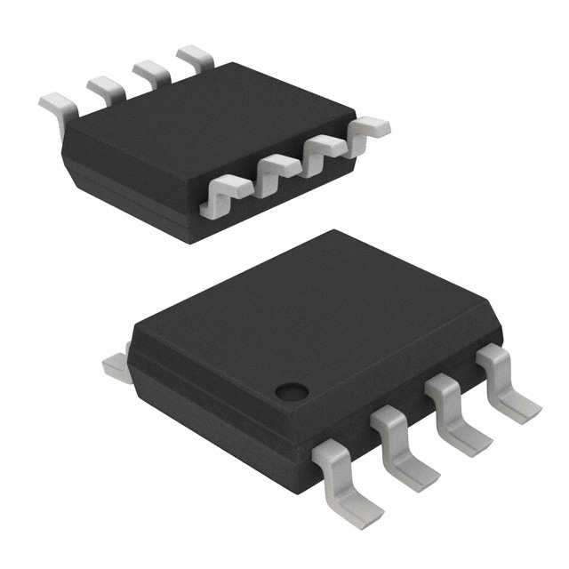
The device is packaged in a surface-mount 8-SOIC (0.154", 3.90mm Width) package. It operates over a junction temperature range of -55°C to 150°C and has a maximum power dissipation of 2.5W at 25°C ambient. The FDS3692 is RoHS3 compliant, Pb-Free, and Halide Free, with a maximum junction-to-ambient thermal resistance of 50°C/W (10s) and 85°C/W (1000s).
| Qty | Low | High |
|---|---|---|
| 1+ | $2.01 | $2.01 |
| 10+ | $1.29 | $1.29 |
| 100+ | $0.86 | $0.86 |
| 2,500+ | $0.86 | $0.86 |
Estimated market price range - modelled values for guidance only, not live distributor offers.
The maximum drain-source voltage is 100 V.
The FDS3692 is available in an 8-SOIC (0.154", 3.90mm Width) surface-mount package.
The operating junction temperature range is -55°C to 150°C.
Yes, it is RoHS3 compliant, Pb-Free, and Halide Free as per the datasheet.
The continuous drain current is 4.5 A at 25°C ambient temperature.
The maximum on-resistance is 60 mΩ at Vgs = 10 V, Id = 4.5 A, with a typical value of 50 mΩ.
The typical total gate charge is 11 nC at Vgs = 10 V.