

| Distributor | Stock | Pricing | MOQ | PKG | Lead Time | Date Code | On Order Quantity | On Order Delivery | |
|---|---|---|---|---|---|---|---|---|---|
|
290 pcs
|
290 pcs | On Request | 1 | On Request | On Request | 11+ | On Request | On Request | |
|
22 pcs
|
22 pcs | On Request | 1 | On Request | On Request | 11+ | On Request | On Request |
| Category | |
| Manufacturer Name | |
| Configuration | |
| Current | |
| Drain Current Continuous (@ Q 1) | |
| Drain Current Continuous (@ Q 2) | |
| Drain Current, Pulsed | |
| Drain Source On Resistance (Minimum/Typical/Maximum @ Q 1, VGS=10 V, ID=11 A) | |
| Drain Source On Resistance (Minimum/Typical/Maximum @ Q 1, VGS=4.5 V, ID=10 A) | |
| Drain Source On Resistance (Minimum/Typical/Maximum @ Q 2, VGS=10 V, ID=14 A) | |
| Drain Source On Resistance (Minimum/Typical/Maximum @ Q 2, VGS=4.5 V, ID=13 A) | |
| Drain to Source Voltage (Vdss) | |
| FET Feature | |
| Gate Charge (Qg) (Max) @ Vgs | |
| Gate Resistance (@ Q 1, VGS=15 mV, f=1 MHz) | |
| Gate Resistance (@ Q 2, VGS=15 mV, f=1 MHz) | |
| Gate Threshold Voltage (Minimum/Typical/Maximum @ Q 1, VDS=VGS, ID=250 µA) | |
| Gate Threshold Voltage (Minimum/Typical/Maximum @ Q 2, VDS=VGS, ID=1 mA) | |
| Input Capacitance (@ Q 1, VDS=15 V, VGS=0 V, f=1 MHz) | |
| Input Capacitance (@ Q 2, VDS=15 V, VGS=0 V, f=1 MHz) | |
| Input Capacitance (Ciss) (Max) @ Vds | |
| Mounting Type | |
| Operating Temperature | |
| Output Capacitance (@ Q 1, VDS=15 V, VGS=0 V, f=1 MHz) | |
| Output Capacitance (@ Q 2, VDS=15 V, VGS=0 V, f=1 MHz) | |
| Power | |
| Power Dissipation (@ Q 1, Note 1 a&1 b) | |
| Power Dissipation (@ Q 1, Note 1 c&1 d) | |
| Power Dissipation (@ Q 2, Note 1 a&1 b) | |
| Power Dissipation (@ Q 2, Note 1 c&1 d) | |
| Rds On (Max) @ Id, Vgs | |
| Reverse Transfer Capacitance (@ Q 1, VDS=15 V, VGS=0 V, f=1 MHz) | |
| Reverse Transfer Capacitance (@ Q 2, VDS=15 V, VGS=0 V, f=1 MHz) | |
| Storage Temperature | |
| Supplier Device Package | |
| Tape & Reel | |
| Technology | |
| Thermal Resistance Junction To Ambient (@ Q 1, Note 1 a&1 b) | |
| Thermal Resistance Junction To Ambient (@ Q 1, Note 1 c&1 d) | |
| Thermal Resistance Junction To Ambient (@ Q 2, Note 1 a&1 b) | |
| Thermal Resistance Junction To Ambient (@ Q 2, Note 1 c&1 d) | |
| Vgs(th) (Max) @ Id |
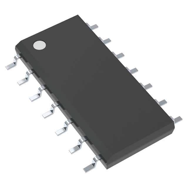
The FDQ7238AS is a dual N-Channel PowerTrench MOSFET designed to replace two single SO-8 MOSFETs in DC to DC power supplies. The high-side switch (Q1) is optimized for reducing switching losses while the low-side switch (Q2) is optimized to reduce conduction losses using Fairchild's SyncFET technology. It includes a patented combination of a MOSFET monolithically integrated with a Schottky diode.
Key electrical specifications include a drain-source voltage of 30V for both MOSFETs. Q2 supports a continuous drain current of 14A with a typical on-resistance of 8.7 mOhm at VGS=10V, while Q1 supports 11A with a typical on-resistance of 13.2 mOhm at VGS=10V. Both devices feature logic level gate drive and a gate threshold voltage range of 1V to 3V.
The device is housed in a 14-SOIC (0.154", 3.90mm Width) surface mount package. It operates over a junction temperature range of -55°C to 150°C. Power dissipation depends on mounting conditions, with Q2 rated up to 2.4W and Q1 up to 1.8W under certain conditions. Thermal resistance junction-to-ambient ranges from 52°C/W to 118°C/W depending on the MOSFET and mounting notes.
| Qty | Low | High |
|---|---|---|
| 245+ | $1.22 | $1.22 |
Estimated market price range - modelled values for guidance only, not live distributor offers.
The drain-source voltage (Vdss) is 30V for both MOSFETs.
It is available in a 14-SOIC (0.154", 3.90mm Width) surface mount package.
The operating junction temperature range is -55°C to 150°C.
Q2 has a continuous drain current of 14A.
The typical on-resistance for Q1 at VGS=10V and ID=11A is 13 mOhm.
Yes, the FET feature is logic level gate, allowing drive at lower gate voltages.