

| Distributor | Stock | Pricing | MOQ | PKG | Lead Time | Date Code | On Order Quantity | On Order Delivery | |
|---|---|---|---|---|---|---|---|---|---|
|
3,000 pcs
|
3000 pcs | On Request | 1 | On Request | On Request | On Request | On Request | On Request | |
|
77 pcs
|
77 pcs | On Request | 1 | On Request | On Request | On Request | On Request | On Request |
| Category | |
| Manufacturer Name | |
| Configuration | |
| Current | |
| Drain to Source Voltage (Vdss) | |
| FET Feature | |
| Gate Charge (Qg) (Max) @ Vgs | |
| Input Capacitance (Ciss) (Max) @ Vds | |
| Mounting Type | |
| Operating Temperature | |
| Power | |
| Rds On (Max) @ Id, Vgs | |
| Supplier Device Package | |
| Tape & Reel | |
| Technology | |
| Vgs(th) (Max) @ Id |
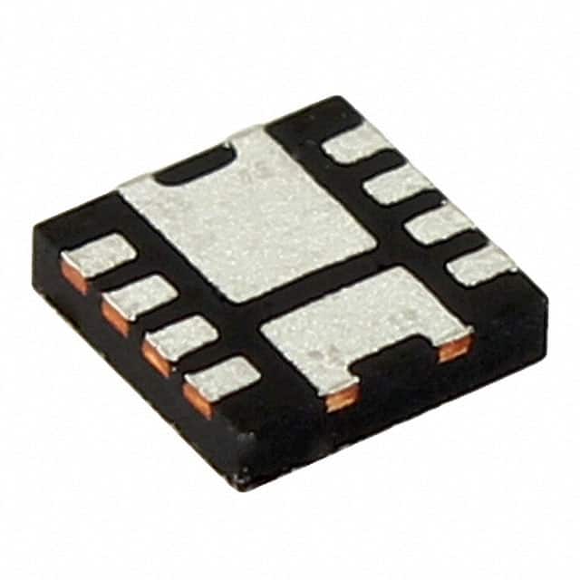
The FDPC8013S is an asymmetric dual N-Channel MOSFET from On Semiconductor, designed for synchronous buck converter applications. It integrates two specialized MOSFETs in a single 8-PowerWDFN (Powerclip-33) package with an internally connected switch node for simplified layout and reduced parasitic inductance. The control MOSFET (Q1) has a maximum on-resistance of 6.4mΩ at 13A and 10V, while the synchronous SyncFET (Q2) achieves 2.7mΩ at 22A and 4.5V. Both channels support a maximum drain-source voltage of 30V. Q1 can handle a continuous drain current of 13A (TA) and 20A (TC), and Q2 can handle 26A (TA) and 55A (TC). Pulse currents are rated at 40A for Q1 and 100A for Q2. The device features a logic level gate with a maximum gate threshold voltage of 3V at 250µA and a total gate charge of 13nC at 10V, enabling efficient switching. Input capacitance is 827pF at 15V. The package supports surface mount assembly with a 0.65mm lead pitch and is supplied on tape and reel (3000 pieces per reel). On-resistance characteristics are also specified at 4.5V gate drive for low-voltage logic compatibility. The device is RoHS compliant and suitable for computing, communications, and general point-of-load power applications.
| Qty | Low | High |
|---|---|---|
| 1+ | $2.68 | $2.68 |
| 10+ | $1.73 | $1.73 |
| 100+ | $1.19 | $1.19 |
| 500+ | $0.95 | $0.95 |
| 1,000+ | $0.84 | $0.84 |
| 3,000+ | $0.83 | $0.83 |
Estimated market price range - modelled values for guidance only, not live distributor offers.
The operating temperature range is -55°C to 150°C (junction temperature).
It is housed in an 8-PowerWDFN package with a supplier device package of Powerclip-33.
Yes, the datasheet states it is RoHS compliant.
The maximum drain-source voltage is 30V for both MOSFETs.
At TA = 25°C, Q1 is rated 13A and Q2 is rated 26A. At TC = 25°C, Q1 is 20A and Q2 is 55A.