

| Distributor | Stock | Pricing | MOQ | PKG | Lead Time | Date Code | On Order Quantity | On Order Delivery | |
|---|---|---|---|---|---|---|---|---|---|
|
51,039 pcs
|
51039 pcs | On Request | 1 | On Request | On Request | On Request | On Request | On Request | |
|
2,264 pcs
|
2264 pcs | On Request | 1 | On Request | On Request | On Request | On Request | On Request | |
|
970 pcs
|
970 pcs | On Request | 1 | On Request | On Request | 17+ | On Request | On Request |
| Category | |
| Manufacturer Name | |
| Configuration | |
| Current | |
| Drain to Source Voltage (Vdss) | |
| FET Feature | |
| Gate Charge (Qg) (Max) @ Vgs | |
| Halogen Free | |
| Input Capacitance (Ciss) (Max) @ Vds | |
| Mounting Type | |
| Operating Temperature | |
| Power | |
| Rds On (Max) @ Id, Vgs | |
| Supplier Device Package | |
| Tape & Reel | |
| Technology | |
| Vgs(th) (Max) @ Id |
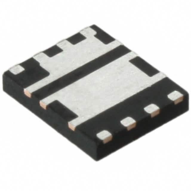
The FDMS3664S is a dual N-Channel asymmetric MOSFET from On Semiconductor, housed in a PQFN8 Power56 package. The switch node is internally connected to simplify layout of synchronous buck converters. The control MOSFET (Q1) and SyncFET (Q2) are optimized for high efficiency.
Key electrical specifications include a maximum drain-to-source voltage of 30V. Q1 supports continuous drain current of 13A at TA=25°C (30A at TC=25°C package limited), while Q2 supports 25A at TA=25°C (60A at TC=25°C package limited). On-resistance is 8mΩ max for Q1 at Vgs=10V and 2.6mΩ max for Q2 at Vgs=10V. Gate charge is 29nC at Vgs=10V, and input capacitance is 1765pF at Vds=15V.
Thermal characteristics include an operating junction temperature range of -55°C to 150°C. Thermal resistance junction-to-case is 2.9°C/W for Q1 and 2.3°C/W for Q2. Power dissipation varies by mounting condition, with maximum values of 2.2W (Q1) and 2.5W (Q2) under certain conditions.
The device is surface mount, RoHS3 compliant, Pb-Free, and Halide Free. It is suitable for computing, communications, and general point-of-load applications, including notebook VCORE regulation.
| Qty | Low | High |
|---|---|---|
| 1+ | $1.73 | $1.73 |
| 10+ | $1.36 | $1.36 |
| 100+ | $0.98 | $0.98 |
| 500+ | $0.78 | $0.78 |
| 1,000+ | $0.64 | $0.64 |
| 3,000+ | $0.56 | $0.56 |
| 9,000+ | $0.56 | $0.56 |
Estimated market price range - modelled values for guidance only, not live distributor offers.
The maximum drain-to-source voltage is 30 V for both Q1 and Q2.
The device is housed in an 8-PowerTDFN package (Power56).
The operating junction temperature range is -55°C to 150°C.
Yes, the device is RoHS3 compliant, Pb-Free, and Halide Free as per the datasheet.
At TA=25°C, Q1 has a maximum continuous drain current of 13 A, and Q2 has 25 A. At TC=25°C (package limited), Q1 is 30 A and Q2 is 60 A.
The maximum Rds(on) for Q1 at Vgs=10V and Id=13A is 8 mΩ.
The maximum gate threshold voltage is 2.7 V at Id=250 µA.