

| Distributor | Stock | Pricing | MOQ | PKG | Lead Time | Date Code | On Order Quantity | On Order Delivery | |
|---|---|---|---|---|---|---|---|---|---|
|
396,737 pcs
|
396737 pcs | On Request | 1 | On Request | On Request | On Request | On Request | On Request |
| Category | |
| Manufacturer Name | |
| Configuration | |
| Current | |
| Drain to Source Voltage (Vdss) | |
| FET Feature | |
| Gate Charge (Qg) (Max) @ Vgs | |
| Halogen Free | |
| Input Capacitance (Ciss) (Max) @ Vds | |
| Mounting Type | |
| Operating Temperature | |
| Power | |
| Rds On (Max) @ Id, Vgs | |
| Storage Temperature | |
| Supplier Device Package | |
| Tape & Reel | |
| Technology | |
| Vgs(th) (Max) @ Id |
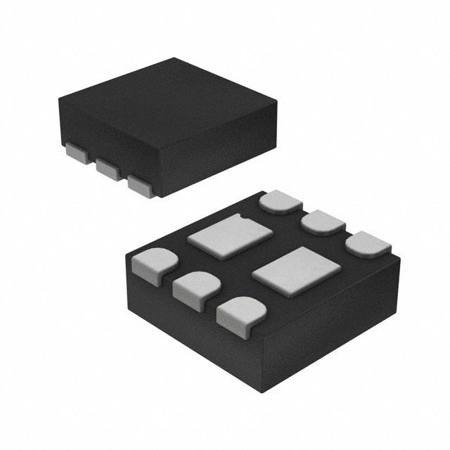
This device is designed specifically as a single package solution for the battery charge switch in cellular handset and other ultra‑portable applications. It features two independent P‑Channel MOSFETs with low on‑state resistance for minimum conduction losses. When connected in the typical common source configuration, bi‑directional current flow is possible. The MicroFET 1.6x1.6 Thin package offers exceptional thermal performance for its physical size and is well suited to switching and linear mode applications.
Key electrical specifications include a maximum drain-source voltage of -20V, continuous drain current of -2.6A at TA=25°C, and pulsed drain current of -6A. On-resistance is specified at multiple gate voltages: 142mΩ at VGS=-4.5V, 213mΩ at -2.5V, 331mΩ at -1.8V, and 530mΩ at -1.5V. Gate threshold voltage is 1V maximum at ID=250µA. Input capacitance is 405pF at VDS=10V, and gate charge is 7.7nC at VGS=4.5V. The device features a logic level gate for direct drive from low-voltage controllers.
Thermal characteristics: power dissipation for single operation is 1.4W (Note 1a) and 0.6W (Note 1b) at TA=25°C. Thermal resistance junction-to-ambient is 90°C/W (Note 1a) and 195°C/W (Note 1b). Operating junction temperature range is -55°C to 150°C.
The device is housed in a 6-UFDFN Exposed Pad package (6-MicroFET 1.6x1.6) for surface mount assembly. It is RoHS3 compliant, Pb-Free, and Halide Free. Typical applications include load switching, battery charging, and battery disconnect switches in portable electronics.
| Qty | Low | High |
|---|---|---|
| 1+ | $1.78 | $1.78 |
| 10+ | $1.10 | $1.10 |
| 100+ | $0.72 | $0.72 |
| 500+ | $0.57 | $0.57 |
| 1,000+ | $0.49 | $0.49 |
| 2,500+ | $0.38 | $0.38 |
| 5,000+ | $0.32 | $0.32 |
| 25,000+ | $0.32 | $0.32 |
Estimated market price range - modelled values for guidance only, not live distributor offers.
-20 V
-2.6 A at TA=25°C
142 mΩ maximum
-55°C to 150°C junction temperature
Yes, RoHS3 compliant, Pb-Free and Halide Free
6-UFDFN Exposed Pad (6-MicroFET 1.6x1.6)
Maximum 1V at ID=250µA