

| Distributor | Stock | Pricing | MOQ | PKG | Lead Time | Date Code | On Order Quantity | On Order Delivery | |
|---|---|---|---|---|---|---|---|---|---|
|
4,020 pcs
|
4020 pcs | On Request | 1 | On Request | On Request | On Request | On Request | On Request |
| Category | |
| Manufacturer Name | |
| Current | |
| Drain to Source Voltage (Vdss) | |
| Drive Voltage (Max Rds On, Min Rds On) | |
| FET Type | |
| Gate Charge (Qg) (Max) @ Vgs | |
| Halogen Free | |
| Input Capacitance (Ciss) (Max) @ Vds | |
| Mounting Type | |
| Operating Temperature | |
| Power Dissipation (Max) | |
| Rds On (Max) @ Id, Vgs | |
| Storage Temperature | |
| Supplier Device Package | |
| Tape & Reel | |
| Technology | |
| Vgs (Max) | |
| Vgs(th) (Max) @ Id |
The FDMC8651 is a 30V N-Channel Power MOSFET from On Semiconductor, built with POWERTRENCH technology. It is optimized for low voltage DC/DC converters, offering low gate charge (27.2 nC at 4.5V) and low input capacitance (3365 pF at 15V) to reduce switching losses. The device supports both 2.5V and 4.5V gate drive voltages, with on-resistance specified at 6.1 mΩ max at 15A, 4.5V, and 9.3 mΩ max at 12A, 2.5V.
For current handling, the package-limited continuous drain current is 20A at Tc=25°C, while the silicon-limited rating is 64A. Pulsed drain current is rated at 60A. The device is 100% UIL tested with an avalanche energy rating of 128 mJ. Power dissipation is 41W at Tc=25°C and 2.3W at Ta=25°C.
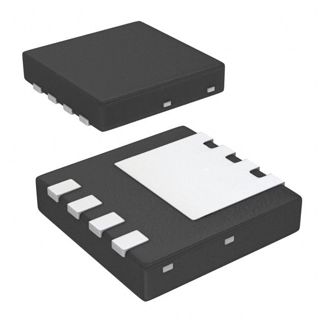
The FDMC8651 is housed in a compact Power33 surface mount package (8-PowerTDFN, PQFN8 3.3x3.3mm) with a low profile of 1 mm max. It is Pb-Free, Halide Free, and RoHS compliant. Typical applications include synchronous rectifiers and 3.3V input synchronous buck converters.
| Qty | Low | High |
|---|---|---|
| 1+ | $2.30 | $2.30 |
| 10+ | $1.46 | $1.46 |
| 100+ | $0.98 | $0.98 |
| 3,000+ | $0.98 | $0.98 |
Estimated market price range - modelled values for guidance only, not live distributor offers.
The maximum drain-source voltage is 30 V.
The device is available in an 8-PowerTDFN (PQFN8) package, also known as Power33, with a 1 mm max profile.
The junction temperature range is -55°C to +150°C.
Yes, it is RoHS3 compliant, Pb-Free and Halide Free as per the datasheet.
The continuous drain current is 20 A at Tc=25°C (package limited), 64 A silicon limited at Tc=25°C, and 15 A at Ta=25°C.
The maximum Rds(on) is 6.1 mΩ at Vgs=4.5V, Id=15A, and 9.3 mΩ at Vgs=2.5V, Id=12A.
The maximum gate charge is 27.2 nC at Vgs=4.5V.