

| Distributor | Stock | Pricing | MOQ | PKG | Lead Time | Date Code | On Order Quantity | On Order Delivery | |
|---|---|---|---|---|---|---|---|---|---|
|
4,514 pcs
|
4514 pcs | On Request | 1 | On Request | On Request | On Request | On Request | On Request |
| Category | |
| Manufacturer Name | |
| Current | |
| Drain to Source Voltage (Vdss) | |
| Drive Voltage (Max Rds On, Min Rds On) | |
| FET Type | |
| Gate Charge (Qg) (Max) @ Vgs | |
| Input Capacitance (Ciss) (Max) @ Vds | |
| Mounting Type | |
| Operating Temperature | |
| Power Dissipation (Max) | |
| Rds On (Max) @ Id, Vgs | |
| Storage Temperature | |
| Supplier Device Package | |
| Tape & Reel | |
| Technology | |
| Vgs (Max) | |
| Vgs(th) (Max) @ Id |
The FDMC8010ET30 is a single N-Channel MOSFET from ON Semiconductor, built using advanced POWERTRENCH technology to achieve extremely low on-resistance. With a maximum drain-source voltage of 30V and continuous drain current of 174A (at Tc=25°C), this device is designed for high-current switching applications where space is limited.
Key electrical characteristics include a maximum Rds(on) of 1.3mΩ at Vgs=10V and 30A, and 1.8mΩ at Vgs=4.5V and 25A. Total gate charge is 94nC at 10V, and input capacitance is 5860pF at 15V. The device can handle pulsed drain currents up to 835A and single pulse avalanche energy of 153mJ. Power dissipation is rated at 65W at Tc=25°C and 2.8W at Ta=25°C.
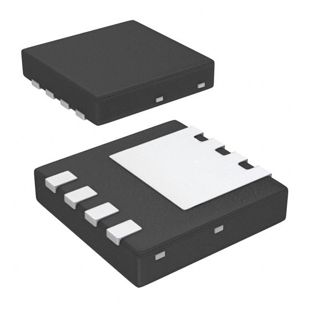
Packaged in a compact 8-PowerWDFN surface mount package (Power33), the FDMC8010ET30 occupies minimal board space while offering excellent thermal performance with junction-to-case thermal resistance of 1.3°C/W. It operates over a junction temperature range of -55°C to 175°C, making it suitable for demanding environments.
Typical applications include DC-DC buck converters, point-of-load regulation, high-efficiency load switches, and ORing FET functions in redundant power systems.
| Qty | Low | High |
|---|---|---|
| 3,000+ | $0.84 | $0.84 |
Estimated market price range - modelled values for guidance only, not live distributor offers.
The maximum drain-source voltage (Vdss) is 30 V.
The device is housed in an 8-PowerWDFN surface mount package, also known as Power33.
The operating junction temperature range is -55°C to 175°C.
Yes, the datasheet states the device is Pb-Free and RoHS Compliant.
The maximum Rds(on) is 1.3 mΩ at Vgs=10 V and Id=30 A; and 1.8 mΩ at Vgs=4.5 V and Id=25 A.
The maximum total gate charge (Qg) is 94 nC at Vgs=10 V.
The single pulse avalanche energy (EAS) is 153 mJ maximum.