

| Distributor | Stock | Pricing | MOQ | PKG | Lead Time | Date Code | On Order Quantity | On Order Delivery | |
|---|---|---|---|---|---|---|---|---|---|
|
4,020 pcs
|
4020 pcs | On Request | 1 | On Request | On Request | 22+ | On Request | On Request | |
|
1,340 pcs
|
1340 pcs | On Request | 1 | On Request | On Request | On Request | On Request | On Request | |
|
282 pcs
|
282 pcs | On Request | 1 | On Request | On Request | 24+ | On Request | On Request | |
|
168 pcs
|
168 pcs | On Request | 1 | On Request | On Request | On Request | On Request | On Request | |
|
155 pcs
|
155 pcs | On Request | 1 | On Request | On Request | On Request | On Request | On Request | |
|
113 pcs
|
113 pcs | On Request | 1 | On Request | On Request | 15+ | On Request | On Request |
| Category | |
| Manufacturer Name | |
| Current | |
| Drain to Source Voltage (Vdss) | |
| Drive Voltage (Max Rds On, Min Rds On) | |
| FET Type | |
| Gate Charge (Qg) (Max) @ Vgs | |
| Halogen Free | |
| Input Capacitance (Ciss) (Max) @ Vds | |
| Mounting Type | |
| Operating Temperature | |
| Power Dissipation (Max) | |
| Rds On (Max) @ Id, Vgs | |
| Supplier Device Package | |
| Tape & Reel | |
| Technology | |
| Vgs (Max) | |
| Vgs(th) (Max) @ Id |
The FDMC2523P is a P-Channel enhancement mode power MOSFET designed and manufactured by On Semiconductor using advanced planar stripe DMOS technology. This device is tailored for applications requiring efficient switching and high energy handling.
Key electrical characteristics include a maximum drain-source voltage of 150V, continuous drain current of 3A (Tc=25°C), and a drain-source on-resistance of 1.5 Ohm at Vgs=-10V, Id=-1.5A. The gate threshold voltage is 5V at Id=250µA, and the maximum gate-source voltage is ±30V. The device exhibits low gate charge (typical 6.2nC) and low reverse transfer capacitance (typical 10pF), supporting fast switching performance.
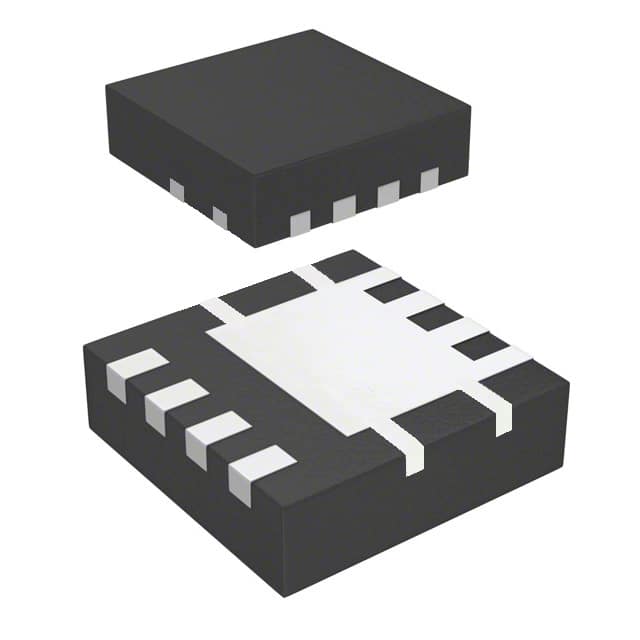
Packaged in a surface mount 8-PowerWDFN (8-MLP 3.3x3.3) case, the FDMC2523P is supplied in tape and reel packaging with a standard quantity of 3000 pieces. The operating junction temperature range is -55°C to +150°C, with a maximum power dissipation of 42W at Tc=25°C.
| Qty | Low | High |
|---|---|---|
| 1+ | $2.63 | $2.63 |
| 10+ | $1.69 | $1.69 |
| 100+ | $1.15 | $1.15 |
| 3,000+ | $1.15 | $1.15 |
Estimated market price range - modelled values for guidance only, not live distributor offers.
The maximum drain-source voltage (Vdss) is 150V.
The continuous drain current is 3A at Tc=25°C, and 1.8A at Tc=100°C.
The operating junction temperature range is -55°C to +150°C.
Yes, the FDMC2523P is RoHS3 compliant, Pb-Free, and Halogen Free/BFR Free.
The FDMC2523P is supplied in an 8-PowerWDFN surface mount package, also designated as 8-MLP (3.3x3.3).
The typical gate charge is 6.2nC at Vgs=10V.