

| Distributor | Stock | Pricing | MOQ | PKG | Lead Time | Date Code | On Order Quantity | On Order Delivery | |
|---|---|---|---|---|---|---|---|---|---|
|
2,600 pcs
|
2600 pcs | On Request | 1 | On Request | On Request | On Request | On Request | On Request |
| Category | |
| Manufacturer Name | |
| Current | |
| Drain to Source Voltage (Vdss) | |
| Drive Voltage (Max Rds On, Min Rds On) | |
| FET Type | |
| Gate Charge (Qg) (Max) @ Vgs | |
| Input Capacitance (Ciss) (Max) @ Vds | |
| Medical Grade | |
| Mounting Type | |
| Operating Temperature | |
| Power Dissipation (Max) | |
| Rds On (Max) @ Id, Vgs | |
| Supplier Device Package | |
| Tape & Reel | |
| Technology | |
| Vgs (Max) | |
| Vgs(th) (Max) @ Id |
The FDMC2512SDC is an N-Channel enhancement-mode power MOSFET designed for high-efficiency power conversion applications. Manufactured by ON Semiconductor, this device utilizes advanced MOSFET technology to achieve a maximum drain-source voltage of 25V and a continuous drain current of up to 40A at case temperature (Tc) or 32A at ambient temperature (Ta).
The MOSFET offers an ultra-low on-resistance of 2mOhm maximum when driven with 10V at 27A, minimizing conduction losses. The gate threshold voltage is 2.5V maximum at 1mA drain current, and the recommended gate drive range is 4.5V to 10V. Input capacitance is 4410pF typical at 13V Vds, and total gate charge is 68nC at 10V.
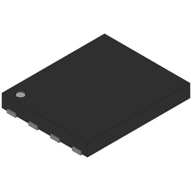
Housed in an 8-PowerTDFN surface mount package with supplier device package 8-PQFN (3.3x3.3 mm), this device is suitable for compact power management designs. Maximum power dissipation is 3W at ambient temperature and 66W at case temperature. Operating junction temperature ranges from -55°C to 150°C.
The maximum drain-source voltage (Vdss) is 25V.
The maximum drain current is 40A at case temperature (Tc) and 32A at ambient temperature (Ta).
The maximum on-resistance is 2mOhm at a drain current of 27A with a gate voltage of 10V.
It is supplied in an 8-PowerTDFN surface mount package (8-PQFN 3.3x3.3mm).
The junction temperature range is -55°C to 150°C.
The device is reported as RoHS3 compliant and REACH unaffected, but this data is unverified.