

| Distributor | Stock | Pricing | MOQ | PKG | Lead Time | Date Code | On Order Quantity | On Order Delivery | |
|---|---|---|---|---|---|---|---|---|---|
|
19,020 pcs
|
19020 pcs | On Request | 1 | On Request | On Request | On Request | On Request | On Request | |
|
1,230 pcs
|
1230 pcs | On Request | 1 | On Request | On Request | On Request | On Request | On Request |
| Category | |
| Manufacturer Name | |
| Current | |
| Drain to Source Voltage (Vdss) | |
| Drive Voltage (Max Rds On, Min Rds On) | |
| FET Type | |
| Gate Charge (Qg) (Max) @ Vgs | |
| Halogen Free | |
| Input Capacitance (Ciss) (Max) @ Vds | |
| Mounting Type | |
| Operating Temperature | |
| Power Dissipation (Max) | |
| Rds On (Max) @ Id, Vgs | |
| SVHC Present | |
| Supplier Device Package | |
| Tape & Reel | |
| Technology | |
| Vgs (Max) | |
| Vgs(th) (Max) @ Id |
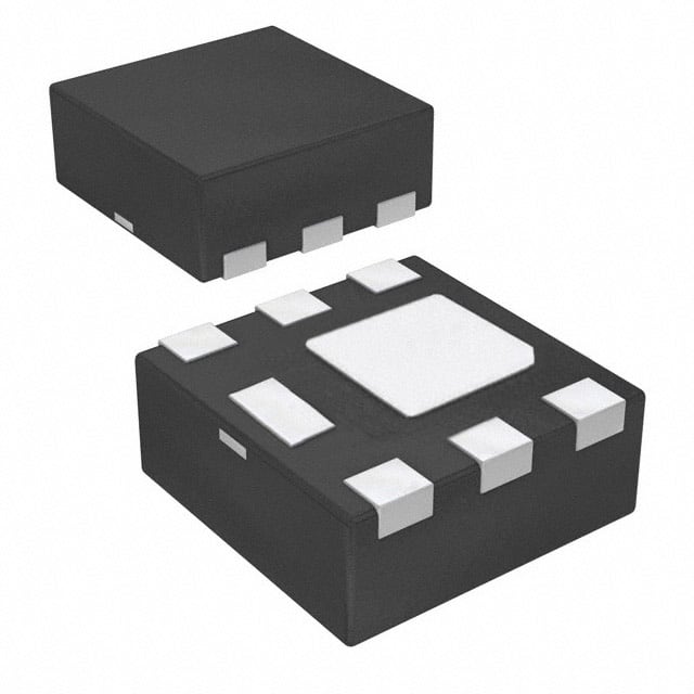
The FDMA507PZ is a P-Channel MOSFET from On Semiconductor, designed for battery charge and load switching in cellular handsets and other ultraportable applications. It features low on-state resistance and is part of the POWERTRENCH family.
Key electrical specifications include a maximum drain-source voltage of 20V, continuous drain current of 7.8A at 25°C ambient, and low on-resistance: 24mOhm maximum at VGS=5V (ID=7.8A), 25mOhm at 4.5V, 35mOhm at 2.5V, and 45mOhm at 1.8V. The gate threshold voltage is 0.5V typical (1.5V maximum), and the gate charge is 42nC at 5V. Input capacitance is 2015pF at VDS=10V.
The device is housed in a 6-WDFN exposed pad package (MicroFET 2x2) and is surface mountable. Thermal resistance from junction to ambient is 52°C/W (Note 1a) and 145°C/W (Note 1b), with maximum power dissipation of 2.4W at 25°C. Operating junction temperature range is -55°C to 150°C.
The FDMA507PZ is Pb-Free, Halogen Free, and RoHS compliant per the datasheet. It also features HBM ESD protection greater than 3.2kV typical. This MOSFET is suitable for linear mode applications due to its excellent thermal performance in a small package.
| Qty | Low | High |
|---|---|---|
| 1+ | $1.07 | $1.07 |
| 10+ | $0.67 | $0.67 |
| 100+ | $0.44 | $0.44 |
| 500+ | $0.34 | $0.34 |
| 3,000+ | $0.34 | $0.34 |
Estimated market price range - modelled values for guidance only, not live distributor offers.
The drain-source voltage rating is 20V maximum.
It is available in a 6-WDFN exposed pad package, also known as MicroFET (2x2).
The operating junction temperature range is -55°C to 150°C.
Yes, the device is RoHS compliant and Pb-Free as per the datasheet.
Continuous drain current is 7.8A at 25°C ambient.
Maximum on-resistance is 24mOhm at VGS=5V and ID=7.8A.