

| Distributor | Stock | Pricing | MOQ | PKG | Lead Time | Date Code | On Order Quantity | On Order Delivery | |
|---|---|---|---|---|---|---|---|---|---|
|
6,000 pcs
|
6000 pcs | On Request | 1 | On Request | On Request | 21+ | On Request | On Request | |
|
5,491 pcs
|
5491 pcs | On Request | 1 | On Request | On Request | 21+ | On Request | On Request | |
|
4,500 pcs
|
4500 pcs | On Request | 1 | On Request | On Request | On Request | On Request | On Request | |
|
4,000 pcs
|
4000 pcs | On Request | 1 | On Request | On Request | On Request | On Request | On Request | |
|
465 pcs
|
465 pcs | On Request | 1 | On Request | On Request | On Request | On Request | On Request |
| Category | |
| Manufacturer Name | |
| Configuration | |
| Conflict Minerals | |
| Current | |
| Drain to Source Voltage (Vdss) | |
| FET Feature | |
| Gate Charge (Qg) (Max) @ Vgs | |
| Halogen Free | |
| Input Capacitance (Ciss) (Max) @ Vds | |
| Mounting Type | |
| Operating Temperature | |
| Power | |
| Rds On (Max) @ Id, Vgs | |
| SVHC Present | |
| Supplier Device Package | |
| Tape & Reel | |
| Technology | |
| Vgs(th) (Max) @ Id |
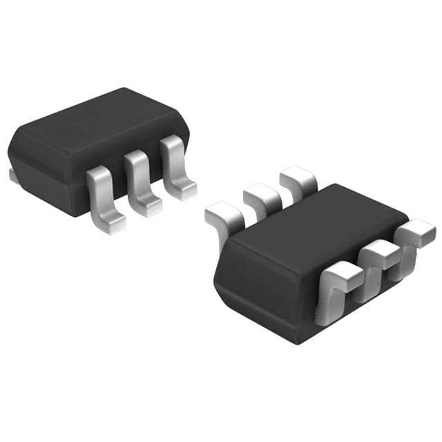
The FDG8850NZ is a dual N-Channel logic level enhancement mode MOSFET from On Semiconductor, manufactured using PowerTrench DMOS technology. This device is designed for low voltage applications and can replace bipolar digital transistors and small signal MOSFETs. It offers a maximum drain-source voltage of 30V and a continuous drain current of 0.75A per channel. The on-resistance is typically 0.4Ω maximum at VGS=4.5V and ID=0.75A, and 0.5Ω maximum at VGS=2.7V and ID=0.67A. The gate threshold voltage is 1.5V maximum at ID=250µA, enabling operation in 3V circuits. The device features a logic level gate, allowing direct drive from low-voltage logic. The FDG8850NZ is housed in a compact SC-88 (SC-70-6) surface-mount package, which is lead-free, halide-free, and RoHS compliant. It is rated for operating junction temperatures from -55°C to +150°C. The maximum power dissipation is 0.36W (note 1a) and 0.3W (note 1b). The input capacitance is 120pF maximum at VDS=10V, and the gate charge is 1.44nC maximum at VGS=4.5V. This dual MOSFET is suitable for load switching, power management, and other low-voltage applications where space is at a premium.
| Qty | Low | High |
|---|---|---|
| 1+ | $0.83 | $0.83 |
Estimated market price range - modelled values for guidance only, not live distributor offers.
30V.
SC-88 (SC-70-6) surface-mount package.
-55°C to +150°C (junction temperature).
Yes, it is RoHS3 compliant, Pb-free, and Halide-free.
Maximum 0.4Ω at VGS=4.5V, ID=0.75A; 0.5Ω at VGS=2.7V, ID=0.67A.
0.75A per channel.
1.5V maximum at ID=250µA.