

| Distributor | Stock | Pricing | MOQ | PKG | Lead Time | Date Code | On Order Quantity | On Order Delivery | |
|---|---|---|---|---|---|---|---|---|---|
|
543,000 pcs
|
543000 pcs | On Request | 1 | On Request | On Request | On Request | On Request | On Request | |
|
18,361 pcs
|
18361 pcs | On Request | 1 | On Request | On Request | 14+ | On Request | On Request | |
|
4,438 pcs
|
4438 pcs | On Request | 1 | On Request | On Request | 20+ | On Request | On Request | |
|
1,800 pcs
|
1800 pcs | On Request | 1 | On Request | On Request | On Request | On Request | On Request | |
|
259 pcs
|
259 pcs | On Request | 1 | On Request | On Request | On Request | On Request | On Request |
| Category | |
| Manufacturer Name | |
| Configuration | |
| Current | |
| Drain to Source Voltage (Vdss) | |
| FET Feature | |
| Gate Charge (Qg) (Max) @ Vgs | |
| Input Capacitance (Ciss) (Max) @ Vds | |
| Mounting Type | |
| Operating Temperature | |
| Power | |
| Rds On (Max) @ Id, Vgs | |
| Storage Temperature | |
| Supplier Device Package | |
| Tape & Reel | |
| Technology | |
| Vgs(th) (Max) @ Id |
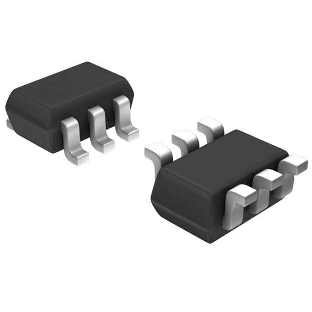
The FDG6320C is a dual N and P-Channel logic level enhancement mode field effect transistor produced by On Semiconductor using their proprietary DMOS technology. This device is designed for low voltage applications and can replace bipolar digital transistors and small signal MOSFETs without requiring bias resistors. The N-Channel MOSFET has a drain-source voltage rating of 25V and a continuous drain current of 220mA, with a pulsed current capability of 650mA. The P-Channel MOSFET has a drain-source voltage rating of -25V and a continuous drain current of -140mA (pulsed -400mA). Gate-source voltage is rated at 8V for N-Channel and -8V for P-Channel. The device features logic level gate drive with a gate threshold voltage of less than 1.5V, allowing direct operation in 3V circuits. On-resistance for the N-Channel at Vgs=4.5V is 4Ω maximum, and for the P-Channel at Vgs=-4.5V is 10Ω maximum. The device also includes a gate-source Zener for ESD ruggedness, rated at 6kV human body model. Power dissipation is 300mW. The FDG6320C is housed in a compact SC-88 (SC-70-6) surface mount package, which is very small and suitable for space-constrained designs. Operating temperature range is -55°C to 150°C. The device is Pb-Free and RoHS compliant (unverified). This dual digital FET is ideal for low voltage portable electronics, load switching, and power management applications.
| Qty | Low | High |
|---|---|---|
| 3,000+ | $1.40 | $1.40 |
Estimated market price range - modelled values for guidance only, not live distributor offers.
The N-Channel MOSFET has a minimum drain-source breakdown voltage of 25V.
The FDG6320C is available in a 6-TSSOP, SC-88, SOT-363 package, specifically the SC-88 (SC-70-6) supplier device package.
The operating temperature range is -55°C to 150°C (junction).
The datasheet claims the device is Pb-Free and RoHS compliant, but this is unverified.
The maximum gate threshold voltage is 1.5V at a drain current of 250µA.
The maximum on-resistance for the N-Channel is 4Ω at Vgs=4.5V and Id=220mA.
Yes, the device has a gate-source Zener for ESD ruggedness, rated at 6kV human body model.