

| Distributor | Stock | Pricing | MOQ | PKG | Lead Time | Date Code | On Order Quantity | On Order Delivery | |
|---|---|---|---|---|---|---|---|---|---|
|
1,000 pcs
|
1000 pcs | On Request | 1 | On Request | On Request | On Request | On Request | On Request |
| Category | |
| Manufacturer Name | |
| Configuration | |
| Current | |
| Drain to Source Voltage (Vdss) | |
| FET Feature | |
| Gate Charge (Qg) (Max) @ Vgs | |
| Halogen Free | |
| Input Capacitance (Ciss) (Max) @ Vds | |
| Mounting Type | |
| Operating Temperature | |
| Power | |
| Rds On (Max) @ Id, Vgs | |
| Supplier Device Package | |
| Tape & Reel | |
| Technology | |
| Vgs(th) (Max) @ Id |
The FDG1024NZ is a dual N-channel logic level enhancement mode MOSFET manufactured by onsemi. It uses a high cell density DMOS process to minimize on-state resistance, making it suitable for low-voltage switching applications. The device can replace bipolar digital transistors and small signal MOSFETs in circuits requiring low gate drive.
Electrical specifications include a 20 V drain-to-source voltage rating, ±8 V maximum gate-to-source voltage, and 1.2 A continuous drain current at 25°C ambient. Pulsed drain current is rated at 6 A. On-resistance is specified as 175 mΩ maximum at VGS = 4.5 V and ID = 1.2 A, and 389 mΩ maximum at VGS = 1.5 V, enabling operation in 1.5 V logic systems. Maximum gate threshold voltage is 1 V at 250 µA, and gate charge is only 2.6 nC at 4.5 V, offering fast switching with low drive requirements.
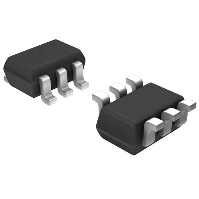
The device is available in the compact SC-88/SC-70-6 surface-mount package (6-TSSOP/SOT-363). It provides HBM ESD protection above 2 kV and is RoHS compliant and halogen free. Power dissipation is rated at 360 mW (mounting note 1a) and 300 mW (note 1b), with junction-to-ambient thermal resistance of 350 °C/W and 415 °C/W, respectively. The operating junction temperature range is -55 °C to +150 °C. With its symmetrical pinout and logic-level gate, the FDG1024NZ is well suited for battery-powered portable electronics and low-voltage white goods.
The FDG1024NZ has a drain-to-source voltage rating of 20 V, with a minimum breakdown voltage of 20 V at ID = 250 µA, VGS = 0 V.
The FDG1024NZ is available in 6-TSSOP, SC-88, SOT-363 packages; the supplier device package is SC-88 (SC-70-6). It is a surface-mount package.
The operating junction temperature range is -55°C to +150°C.
Yes, the datasheet states the device is RoHS compliant and halogen free.
The maximum continuous drain current is 1.2 A at TA = 25°C, with pulsed drain current up to 6 A.
The maximum on-resistance is 175 mΩ at VGS = 4.5 V and ID = 1.2 A.
Yes, the maximum gate threshold voltage is 1 V, and on-resistance is specified at VGS = 1.5 V (389 mΩ max at ID = 0.8 A).