

| Distributor | Stock | Pricing | MOQ | PKG | Lead Time | Date Code | On Order Quantity | On Order Delivery | |
|---|---|---|---|---|---|---|---|---|---|
|
543,000 pcs
|
543000 pcs | On Request | 1 | On Request | On Request | On Request | On Request | On Request |
| Category | |
| Manufacturer Name | |
| Current | |
| Drain to Source Voltage (Vdss) | |
| Drive Voltage (Max Rds On, Min Rds On) | |
| FET Feature | |
| FET Type | |
| Gate Charge (Qg) (Max) @ Vgs | |
| Input Capacitance (Ciss) (Max) @ Vds | |
| Medical Grade | |
| Mounting Type | |
| Operating Temperature | |
| Power Dissipation (Max) | |
| Rds On (Max) @ Id, Vgs | |
| Storage Temperature | |
| Supplier Device Package | |
| Tape & Reel | |
| Technology | |
| Vgs (Max) | |
| Vgs(th) (Max) @ Id |
FDFM2P110 is a P-Channel MOSFET manufactured by On Semiconductor. It features a 20V drain-to-source voltage rating and 3.5A continuous drain current at 25°C ambient. The device has a maximum on-resistance of 140mΩ with 4.5V gate drive, and a gate threshold voltage of 1.5V at 250µA. The MOSFET integrates an isolated Schottky diode for improved switching performance.
The device is built with metal-oxide semiconductor technology and offers a low gate charge of 4nC and input capacitance of 280pF, making it suitable for high-efficiency switching circuits. It can be driven at 2.5V or 4.5V logic levels, with maximum gate-source voltage rated at ±12V.
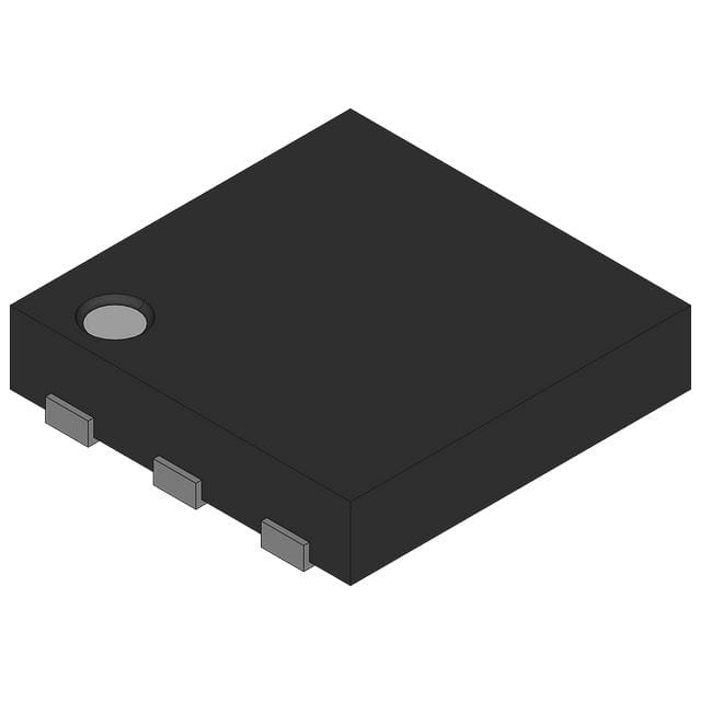
The FDFM2P110 is surface-mount packaged in a 6-WDFN exposed pad package, also known as MicroFET 3x3mm. It supports a maximum power dissipation of 2W at 25°C ambient and operates over a junction temperature range of -55°C to 150°C.
Typical applications include load switches, DC-DC converters, battery management, and portable electronics where low-voltage P-Channel MOSFET switching is required.
| Qty | Low | High |
|---|---|---|
| 3,000+ | $0.23 | $0.23 |
Estimated market price range - modelled values for guidance only, not live distributor offers.
The FDFM2P110 has a drain-to-source voltage rating of 20V.
The maximum continuous drain current is 3.5A at 25°C ambient temperature.
Maximum on-resistance is 140mΩ at Vgs=4.5V and Id=3.5A.
Junction temperature ranges from -55°C to 150°C.
It is available in a 6-WDFN exposed pad package, also known as MicroFET 3x3mm.
The existing data indicates RoHS3 compliance, but this status is unverified and should be confirmed with official documentation.
The maximum gate threshold voltage is 1.5V at a drain current of 250µA.