

| Distributor | Stock | Pricing | MOQ | PKG | Lead Time | Date Code | On Order Quantity | On Order Delivery | |
|---|---|---|---|---|---|---|---|---|---|
|
10,000 pcs
|
10000 pcs | On Request | 1 | On Request | On Request | On Request | On Request | On Request |
| Category | |
| Manufacturer Name | |
| AEC Qualified | |
| Automotive Grade | |
| Current | |
| Drain to Source Voltage (Vdss) | |
| Drive Voltage (Max Rds On, Min Rds On) | |
| FET Type | |
| Gate Charge (Qg) (Max) @ Vgs | |
| Halogen Free | |
| Industrial Grade | |
| Input Capacitance (Ciss) (Max) @ Vds | |
| Medical Grade | |
| Military Grade | |
| Mounting Type | |
| Operating Temperature | |
| Power Dissipation (Max) | |
| Rds On (Max) @ Id, Vgs | |
| SVHC Present | |
| Storage Temperature | |
| Supplier Device Package | |
| Tape & Reel | |
| Tape Width | |
| Technology | |
| Vgs (Max) | |
| Vgs(th) (Max) @ Id |
The FDD8882 is an N-Channel PowerTrench MOSFET from ON Semiconductor designed for high-efficiency power conversion. It is rated for a maximum drain-to-source voltage of 30V and a maximum gate-to-source voltage of ±20V. The device can handle up to 55A of continuous drain current when the case temperature is held at 25°C, with a maximum power dissipation of 55W. At VGS=10V and ID=35A, the maximum drain-to-source on-resistance is 11.5mΩ; at VGS=4.5V, the maximum is 15.0mΩ. Gate threshold voltage ranges from 1.2V to 2.5V.
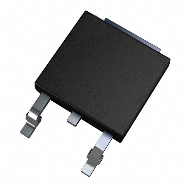
The MOSFET employs high-performance trench technology that provides a low on-resistance and low gate charge. Total gate charge is 22nC typical and 33nC maximum at VGS=10V, supporting fast switching and improved efficiency in DC/DC converter applications. The device is available in a TO-252-3 (DPak) surface-mount package with tape-and-reel packaging of 2500 units per reel.
Typical applications include synchronous and conventional switching PWM controllers used in DC/DC converters. The FDD8882 is also suitable for load switching and other power management circuits requiring a 30V N-Channel MOSFET with high current capability. The junction operating temperature range is -55°C to 175°C.
| Qty | Low | High |
|---|---|---|
| 2,500+ | $0.24 | $0.24 |
Estimated market price range - modelled values for guidance only, not live distributor offers.
The FDD8882 has a maximum drain-to-source voltage of 30V, and a maximum gate-to-source voltage of ±20V.
The FDD8882 is available in a TO-252-3 (DPak, 2 leads + tab) surface-mount package, also specified as TO-252AA.
The junction operating temperature range is -55°C to 175°C.
The datasheet indicates RoHS compliance; however, the compliance status is unverified.
The maximum continuous drain current is 55A at Tc=25°C with VGS=10V, and 12.6A at Tamb=25°C with VGS=10V and RθJA=52°C/W.
The maximum on-resistance is 11.5mΩ at VGS=10V and ID=35A, and 15.0mΩ at VGS=4.5V and ID=35A. Typical values are 9.4mΩ and 13.0mΩ, respectively.
The total gate charge is 22nC typical and 33nC maximum at VGS=10V.