

| Distributor | Stock | Pricing | MOQ | PKG | Lead Time | Date Code | On Order Quantity | On Order Delivery | |
|---|---|---|---|---|---|---|---|---|---|
|
120,533 pcs
|
120533 pcs | On Request | 1 | On Request | On Request | On Request | On Request | On Request | |
|
1,077 pcs
|
1077 pcs | On Request | 1 | On Request | On Request | On Request | On Request | On Request | |
|
1,000 pcs
|
1000 pcs | On Request | 1 | On Request | On Request | On Request | On Request | On Request | |
|
548 pcs
|
548 pcs | On Request | 1 | On Request | On Request | 11+ | On Request | On Request |
| Category | |
| Manufacturer Name | |
| Current | |
| Drain to Source Voltage (Vdss) | |
| Drive Voltage (Max Rds On, Min Rds On) | |
| FET Type | |
| Gate Charge (Qg) (Max) @ Vgs | |
| Input Capacitance (Ciss) (Max) @ Vds | |
| Medical Grade | |
| Mounting Type | |
| Operating Temperature | |
| Power Dissipation (Max) | |
| Rds On (Max) @ Id, Vgs | |
| SVHC Present | |
| Supplier Device Package | |
| Tape & Reel | |
| Technology | |
| Vgs (Max) | |
| Vgs(th) (Max) @ Id |
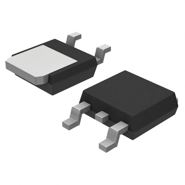
The FDD86250 is an N-Channel power MOSFET manufactured by ON Semiconductor. It is designed for high-efficiency power switching applications. The device has a maximum drain-source voltage (Vdss) of 150V and can handle a continuous drain current of 50A at a case temperature of 25°C (8A at ambient temperature). The on-resistance (Rds(on)) is typically 22mOhm at a gate-source voltage of 10V and drain current of 8A. The gate threshold voltage (Vgs(th)) is 4V maximum at 250µA drain current. The input capacitance (Ciss) is 2110pF at 75V Vds, and the total gate charge (Qg) is 33nC at 10V. The device can dissipate up to 132W at Tc=25°C (3.1W at Ta=25°C). The operating junction temperature range is -55°C to 150°C. The FDD86250 is offered in a DPAK (TO-252) surface mount package, suitable for automated assembly and compact PCB layouts.
| Qty | Low | High |
|---|---|---|
| 1+ | $1.84 | $1.84 |
| 10+ | $1.20 | $1.20 |
| 100+ | $0.92 | $0.92 |
| 2,500+ | $0.92 | $0.92 |
Estimated market price range - modelled values for guidance only, not live distributor offers.
The maximum drain-source voltage (Vdss) is 150V.
The continuous drain current is 50A at Tc=25°C and 8A at Ta=25°C.
The maximum on-resistance (Rds(on)) is 22mOhm at Id=8A and Vgs=10V.
The maximum gate threshold voltage (Vgs(th)) is 4V at Id=250µA.
The operating junction temperature range is -55°C to 150°C.
The FDD86250 is available in a DPAK (TO-252) surface mount package.
The maximum total gate charge (Qg) is 33nC at Vgs=10V.