

| Distributor | Stock | Pricing | MOQ | PKG | Lead Time | Date Code | On Order Quantity | On Order Delivery | |
|---|---|---|---|---|---|---|---|---|---|
|
4,780 pcs
|
4780 pcs | On Request | 1 | On Request | On Request | 12+ | On Request | On Request | |
|
370 pcs
|
370 pcs | On Request | 1 | On Request | On Request | On Request | On Request | On Request |
| Category | |
| Manufacturer Name | |
| Current | |
| Drain to Source Voltage (Vdss) | |
| Drive Voltage (Max Rds On, Min Rds On) | |
| FET Type | |
| Gate Charge (Qg) (Max) @ Vgs | |
| Input Capacitance | |
| Input Capacitance (Ciss) (Max) @ Vds | |
| Mounting Type | |
| Operating Temperature | |
| Package / Case | |
| Power Dissipation (Max) | |
| Rds On (Max) @ Id, Vgs | |
| Supplier Device Package | |
| Tape & Reel | |
| Technology | |
| Vgs (Max) | |
| Vgs(th) (Max) @ Id |
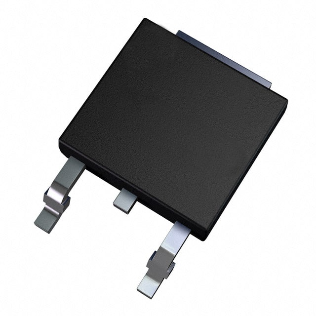
The FDD8586 is an N-Channel PowerTrench MOSFET designed for high-efficiency DC/DC converter applications. It features a maximum drain-source voltage of 20V and continuous drain current of 35A at case temperature 25°C. The device offers low on-resistance: typically 4.0mΩ at VGS=10V and ID=35A, with a maximum of 5.5mΩ. At logic-level gate drive of 4.5V, typical Rds(on) is 5.7mΩ with 8.5mΩ maximum.
This MOSFET is optimized for fast switching with low gate charge (34nC typical at 10V) and low gate resistance (1.2Ω typical). It is 100% avalanche tested with a single pulse avalanche energy rating of 144mJ. The device is RoHS compliant and comes in a surface mount TO-252AA (DPak) package, suitable for automated assembly.
Thermal characteristics include junction-to-case thermal resistance of 1.94°C/W and junction-to-ambient of 100°C/W (TO-252) or 52°C/W with 1in² copper pad. Operating temperature range is -55°C to 175°C. The part is supplied in tape and reel packaging with 2500 units per reel.
| Qty | Low | High |
|---|---|---|
| 568+ | $0.53 | $0.53 |
Estimated market price range - modelled values for guidance only, not live distributor offers.
20V.
35A at case temperature 25°C.
4.0mΩ typical, 5.5mΩ maximum.
-55°C to 175°C junction temperature.
Yes, RoHS3 compliant per datasheet.
Surface mount TO-252AA (DPak).
34nC typical at VGS=10V.