

| Distributor | Stock | Pricing | MOQ | PKG | Lead Time | Date Code | On Order Quantity | On Order Delivery | |
|---|---|---|---|---|---|---|---|---|---|
|
80 pcs
|
80 pcs | On Request | 1 | On Request | On Request | NA | On Request | On Request |
| Category | |
| Manufacturer Name | |
| Current | |
| Drain to Source Voltage (Vdss) | |
| Drive Voltage (Max Rds On, Min Rds On) | |
| FET Type | |
| Gate Charge (Qg) (Max) @ Vgs | |
| Input Capacitance (Ciss) (Max) @ Vds | |
| Lead Style | |
| Mounting Type | |
| Operating Temperature | |
| Power Dissipation (Max) | |
| Rds On (Max) @ Id, Vgs | |
| Supplier Device Package | |
| Technology | |
| Vgs (Max) | |
| Vgs(th) (Max) @ Id |
The FDB86102LZ is an N-Channel MOSFET utilizing metal-oxide semiconductor technology, designed for power management and switching applications. It offers a drain-source voltage rating of 100V and a continuous drain current of up to 30A at case temperature, making it suitable for moderate power circuits.
Key electrical characteristics include a maximum on-resistance of 24 mOhm at a gate voltage of 10V and drain current of 8.3A. The gate charge is 21 nC at 10V, enabling efficient switching, while the input capacitance is 1275 pF at 50V drain-source voltage. The threshold voltage is 3V at 250µA, and recommended drive voltage range is 4.5V to 10V to achieve optimized Rds(on).
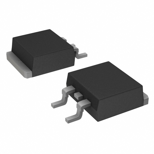
This device is offered in a surface mount TO-263-3 (D²Pak) package, which provides good thermal dissipation in a compact footprint. It operates over a junction temperature range of -55°C to 150°C, with a maximum power dissipation of 3.1W at ambient temperature. The MOSFET is suitable for applications requiring efficient power conversion and load switching in space-constrained designs.
100V.
Surface mount TO-263-3 (D²Pak) package.
-55°C to 150°C junction temperature.
It is listed as RoHS3 Compliant, but this is unverified (low confidence).
24 mOhm at 8.3A drain current and 10V gate voltage.
8.3A at ambient temperature and 30A at case temperature.
21 nC at 10V gate voltage.