

| Distributor | Stock | Pricing | MOQ | PKG | Lead Time | Date Code | On Order Quantity | On Order Delivery | |
|---|---|---|---|---|---|---|---|---|---|
|
258,774 pcs
|
258774 pcs | On Request | 1 | On Request | On Request | On Request | On Request | On Request | |
|
6,413 pcs
|
6413 pcs | On Request | 1 | On Request | On Request | On Request | On Request | On Request | |
|
89 pcs
|
89 pcs | On Request | 1 | On Request | On Request | On Request | On Request | On Request |
| Category | |
| Manufacturer Name | |
| Current | |
| Drain to Source Voltage (Vdss) | |
| Drive Voltage (Max Rds On, Min Rds On) | |
| FET Type | |
| Gate Charge (Qg) (Max) @ Vgs | |
| Halogen Free | |
| Input Capacitance (Ciss) (Max) @ Vds | |
| Mounting Type | |
| Operating Temperature | |
| Power Dissipation (Max) | |
| Rds On (Max) @ Id, Vgs | |
| Supplier Device Package | |
| Tape & Reel | |
| Technology | |
| Termination Style | |
| Vgs (Max) | |
| Vgs(th) (Max) @ Id |
The FDB3652 is an N-Channel Power MOSFET from ON Semiconductor, built with POWERTRENCH technology. It is designed for high-efficiency switching applications including synchronous rectification in ATX, server, and telecom power supplies, battery protection circuits, motor drives, uninterruptible power supplies, and micro solar inverters.
Key electrical ratings include a drain-source breakdown voltage of 100V and continuous drain current of 61A at Tc=25°C (9A at Ta=25°C). The device features low on-resistance: typical 14 mOhm (maximum 16 mOhm) at Vgs=10V, Id=61A. Gate charge is typically 41 nC (maximum 53 nC) at 10V, enabling fast switching. Input capacitance is 2880 pF typical at Vds=25V. The MOSFET is rated for single pulse avalanche energy of 182 mJ.
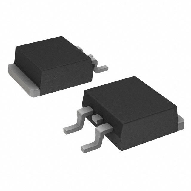
The FDB3652 is offered in a surface mount D2PAK (TO-263-3) package with three leads and a tab for enhanced thermal performance. It operates over a junction temperature range of -55°C to 175°C. Thermal resistance junction-to-case is 1.0°C/W, and junction-to-ambient is 62°C/W (free air) or 43°C/W with a 1 in² copper pad. The device is lead-free and halide-free per the datasheet.
The maximum drain-source voltage (Vdss) is 100 V.
It is available in a TO-263-3 (D²Pak) surface mount package. The supplier device package is D²PAK (TO-263).
The operating junction temperature range is -55°C to 175°C.
The datasheet states it is Pb-Free and Halide Free, and the existing database indicates RoHS3 compliant (unverified).
Maximum on-resistance is 16 mOhm at Vgs=10V, Id=61A. Typical on-resistance is 14 mOhm under the same conditions.
Continuous drain current is 61 A at Tc=25°C with Vgs=10V, and 9 A at Ta=25°C.