

| Distributor | Stock | Pricing | MOQ | PKG | Lead Time | Date Code | On Order Quantity | On Order Delivery | |
|---|---|---|---|---|---|---|---|---|---|
|
7 pcs
|
7 pcs | On Request | 1 | On Request | On Request | On Request | On Request | On Request |
| Category | |
| Manufacturer Name | |
| Current | |
| Drain to Source Voltage (Vdss) | |
| Drive Voltage (Max Rds On, Min Rds On) | |
| FET Type | |
| Gate Charge (Qg) (Max) @ Vgs | |
| Input Capacitance (Ciss) (Max) @ Vds | |
| Mounting Type | |
| Operating Temperature | |
| Power Dissipation (Max) | |
| Rds On (Max) @ Id, Vgs | |
| Supplier Device Package | |
| Technology | |
| Vgs (Max) | |
| Vgs(th) (Max) @ Id |
The FDB2710 is an N-Channel enhancement-mode MOSFET designed and manufactured by ON Semiconductor. This device uses MOSFET (Metal Oxide) technology and is rated for a drain-to-source voltage (Vdss) of 250 V and a continuous drain current (Id) of 50 A at case temperature (Tc). It is suitable for high-power switching applications.
The MOSFET features a low on-resistance of 42.5 mOhm maximum at 25 A gate drive of 10 V. The gate charge (Qg) is 101 nC maximum at Vgs = 10 V, and input capacitance (Ciss) is 7280 pF maximum at Vds = 25 V. The gate threshold voltage (Vgs(th)) is 5 V maximum at 250 µA drain current. Maximum gate-source voltage is ±30 V. The device can dissipate up to 260 W at case temperature (Tc).
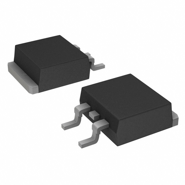
The FDB2710 is offered in a TO-263-3 package, also known as D2Pak (2 Leads + Tab) or TO-263AB. The supplier device package is D2PAK (TO-263). This surface-mount package allows for efficient heat dissipation through the exposed tab. It supports an operating junction temperature range of -55 °C to 150 °C.
This N-Channel MOSFET is designed for applications requiring high efficiency and reliability in power conversion, motor control, and similar circuits. The device is claimed to be RoHS3 compliant, REACH unaffected, and has a Moisture Sensitivity Level (MSL) of 1 (Unlimited), though these compliance claims are currently unverified.
The FDB2710 has a drain-to-source voltage (Vdss) rating of 250 V.
The continuous drain current (Id) is 50 A at case temperature (Tc).
The maximum on-resistance (Rds On) is 42.5 mOhm at Id = 25 A and Vgs = 10 V.
The operating junction temperature range is -55°C to 150°C.
The FDB2710 is offered in a surface-mount D2PAK (TO-263) package.
The FDB2710 is claimed to be RoHS3 compliant, but this status is currently unverified.
The maximum gate charge (Qg) is 101 nC at Vgs = 10 V.