

| Distributor | Stock | Pricing | MOQ | PKG | Lead Time | Date Code | On Order Quantity | On Order Delivery | |
|---|---|---|---|---|---|---|---|---|---|
|
706 pcs
|
706 pcs | On Request | 1 | On Request | On Request | 1032+ | On Request | On Request |
| Category | |
| Manufacturer Name | |
| Current | |
| Drain to Source Voltage (Vdss) | |
| Drive Voltage (Max Rds On, Min Rds On) | |
| FET Type | |
| Gate Charge (Qg) (Max) @ Vgs | |
| Input Capacitance (Ciss) (Max) @ Vds | |
| Lead Style | |
| Mounting Type | |
| Operating Temperature | |
| Power Dissipation (Max) | |
| Rds On (Max) @ Id, Vgs | |
| Storage Temperature | |
| Supplier Device Package | |
| Technology | |
| Vgs (Max) | |
| Vgs(th) (Max) @ Id |
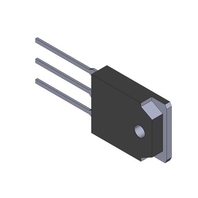
The FDA16N50 is a 500V N-Channel enhancement mode power MOSFET from On Semiconductor, part of the UniFET family. It is designed for high-efficiency switched-mode power supplies and active power factor correction applications.
Key electrical specifications include a continuous drain current of 16.5A at 25°C case temperature, a maximum drain-source on-resistance of 380 mOhm at 8.3A and 10V gate drive, and a total gate charge of 45 nC. The device is rated for a maximum power dissipation of 205W and can operate over a junction temperature range of -55°C to +150°C.
The FDA16N50 is housed in a through-hole TO-3PN package, also known as TO-3P-3 or SC-65-3. It features low input capacitance (1945 pF at 25V) and is 100% avalanche tested, with a single pulsed avalanche energy rating of 780 mJ.
The maximum drain-source voltage (VDSS) is 500V.
The continuous drain current is 16.5A at Tc=25°C and 9.9A at Tc=100°C.
The maximum drain-source on-resistance is 380 mOhm at a drain current of 8.3A and gate-source voltage of 10V.
The FDA16N50 is available in a through-hole TO-3PN package (also known as TO-3P-3 or SC-65-3).
The operating junction temperature range is -55°C to +150°C.
The FDA16N50 is listed as RoHS3 compliant.