

| Distributor | Stock | Pricing | MOQ | PKG | Lead Time | Date Code | On Order Quantity | On Order Delivery | |
|---|---|---|---|---|---|---|---|---|---|
|
67,500 pcs
|
67500 pcs | On Request | 1 | On Request | On Request | On Request | On Request | On Request |
| Category | |
| Manufacturer Name | |
| Current | |
| Drain to Source Voltage (Vdss) | |
| Drive Voltage (Max Rds On, Min Rds On) | |
| FET Type | |
| Gate Charge (Qg) (Max) @ Vgs | |
| Input Capacitance (Ciss) (Max) @ Vds | |
| Mounting Type | |
| Operating Temperature | |
| Power Dissipation (Max) | |
| Rds On (Max) @ Id, Vgs | |
| Supplier Device Package | |
| Tape & Reel | |
| Technology | |
| Vgs (Max) | |
| Vgs(th) (Max) @ Id |
The FCH023N65S3L4 is a high-voltage N-Channel power MOSFET from onsemi's SUPERFET III Easy Drive series, utilizing charge balance technology for low on-resistance and reduced gate charge. It is designed for high-efficiency power conversion in telecom and server power supplies, industrial power supplies, UPS, and solar applications.
Key electrical specifications include a maximum drain-to-source voltage of 650 V, continuous drain current of 75 A at 25°C, and a low typical on-resistance of 19.5 mΩ. The device offers ultra low gate charge (typical 222 nC) and low effective output capacitance (1980 pF), contributing to superior switching performance and reduced switching losses. It is 100% avalanche tested with a single pulsed avalanche energy rating of 2025 mJ.
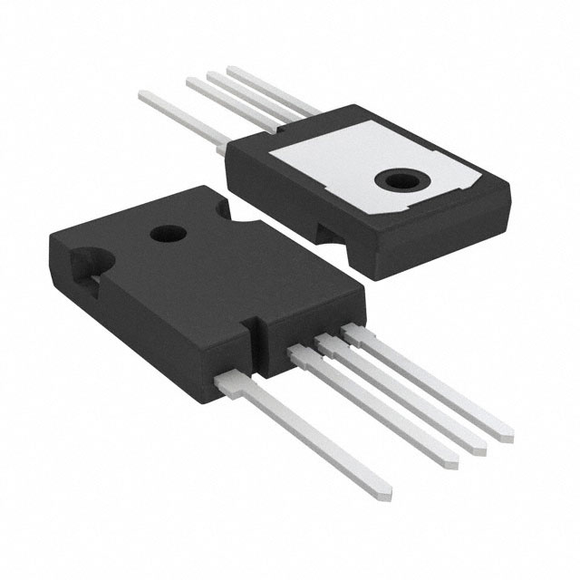
The FCH023N65S3L4 is housed in a TO-247-4 package with through-hole mounting. This package features separate driver and power source pins for optimized gate drive. The device is RoHS compliant and Pb-Free.
| Qty | Low | High |
|---|---|---|
| 1+ | $26.27 | $26.27 |
| 10+ | $18.27 | $18.27 |
Estimated market price range - modelled values for guidance only, not live distributor offers.
The maximum drain-to-source voltage (Vdss) is 650 V.
The maximum continuous drain current at case temperature 25°C is 75 A.
It is available in a TO-247-4 through-hole package.
The operating junction temperature range is -55°C to 150°C.
Yes, the device is RoHS compliant and Pb-Free as stated in the datasheet.
The maximum Rds(on) is 23 mΩ at Vgs = 10 V and Id = 37.5 A.
The single pulsed avalanche energy (EAS) is rated at 2025 mJ at I_AS=15A, RG=25Ω, TJ=25°C.