

| Distributor | Stock | Pricing | MOQ | PKG | Lead Time | Date Code | On Order Quantity | On Order Delivery | |
|---|---|---|---|---|---|---|---|---|---|
|
5,013 pcs
|
5013 pcs | On Request | 1 | On Request | On Request | 18+ | On Request | On Request |
| Category | |
| Manufacturer Name | |
| Configuration | |
| Gate Charge (Qg) (Max) @ Vgs | |
| Halogen Free | |
| Input Capacitance (Ciss) (Max) @ Vds | |
| Mounting Type | |
| Operating Temperature | |
| Power | |
| Storage Temperature | |
| Supplier Device Package | |
| Tape & Reel | |
| Technology | |
| Vgs(th) (Max) @ Id |
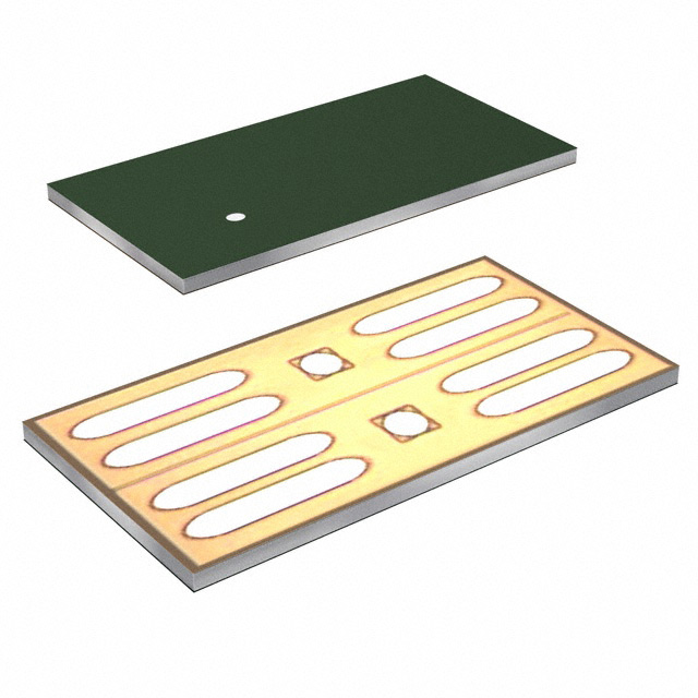
The Panasonic FCAB21490L1 is a dual N-channel MOSFET with an integrated gate resistor, designed specifically for lithium-ion secondary battery protection circuits. It utilizes Chip Size Package (CSP) technology and is halogen-free and RoHS compliant (EU RoHS, UL-94 V-0, MSL Level 1).
Key electrical specifications include a maximum source-source voltage (Vss) of 12V, gate-source voltage range of ±8V, and continuous source current ratings of 13.5A when mounted on an FR4 board (minimum pad size) and 29A on a ceramic substrate. Pulse current capability reaches 135A (10μs, duty ≤1%). The on-state resistance is exceptionally low, with typical values of 2.1mΩ at Vgs=4.5V, 2.2mΩ at Vgs=3.8V, 2.4mΩ at Vgs=3.1V, and 3.1mΩ at Vgs=2.5V (all at Is=6.0A). Gate threshold voltage ranges from 0.35V to 1.4V.
Dynamic characteristics include input capacitance of 3570pF, output capacitance 460pF, reverse transfer capacitance 410pF, and total gate charge of 25nC. Switching times are typical: turn-on delay 0.7μs, rise time 1.5μs, turn-off delay 6.7μs, fall time 4.1μs. The body diode forward voltage is 0.6V minimum, 1.2V maximum.
The device is housed in a 10-SMD, No Lead package (supplier device package 10-SMD) and is surface mountable. Operating channel temperature is up to 150°C, with storage temperature range of -55°C to 150°C. Packaging is embossed tape (thermo-compression sealing) with 1000 pieces per reel.
| Qty | Low | High |
|---|---|---|
| 1,000+ | $0.23 | $0.23 |
Estimated market price range - modelled values for guidance only, not live distributor offers.
20V
13.5A
2.1 mΩ
±8V
3.5W