Ready to onboard?
Are you ready to join DistyParts and
grow your business?


| Distributor | Stock | Pricing | MOQ | PKG | Lead Time | Date Code | On Order Quantity | On Order Delivery | |
|---|---|---|---|---|---|---|---|---|---|
|
7,880,000 pcs
|
7880000 pcs | On Request | 1 | On Request | On Request | On Request | On Request | On Request | |
|
331,020 pcs
|
331020 pcs | On Request | 1 | On Request | On Request | On Request | On Request | On Request | |
|
7,465 pcs
|
7465 pcs | On Request | 1 | On Request | On Request | 16+ | On Request | On Request | |
|
1,000 pcs
|
1000 pcs | On Request | 1 | On Request | On Request | On Request | On Request | On Request |
| Category | |
| Manufacturer Name | |
| Applications | |
| Bidirectional Channels | |
| Capacitance | |
| Capacitance @ Frequency | |
| Clamping Voltage | |
| Current | |
| ESD Air Discharge | |
| ESD Contact Discharge | |
| Halogen Free | |
| IEC 61000-4-5 Peak Pulse Current | |
| Lead Style | |
| Leakage Current | |
| Mounting Type | |
| Operating Temperature | |
| Operating Temperature Range | |
| Package / Case | |
| Package Body Size | |
| Peak Pulse Current | |
| Power Dissipation | |
| Power Line Protection | |
| Supplier Device Package | |
| Tape & Reel | |
| Termination Style | |
| Thermal Resistance Junction-to-Ambient | |
| Type | |
| Voltage | |
| Working Reverse Voltage |
The ESD7181MUT5G is a bidirectional ESD protection diode from On Semiconductor designed to protect voltage sensitive components requiring ultra-low capacitance. It features a working reverse voltage of ±18.5V and a typical clamping voltage of 35V. The device provides IEC 61000-4-2 ESD protection up to 15kV air discharge and 12kV contact discharge, and can handle a peak pulse current of 1A per IEC 61000-4-5 (8/20µs).
With a typical capacitance of only 0.3pF at 1MHz and leakage current below 1nA, this diode is ideal for high-speed signal lines and RF applications where signal integrity is critical. The low dynamic resistance and low insertion loss further enhance its suitability for RF switching, antenna protection, and wireless charger circuits.
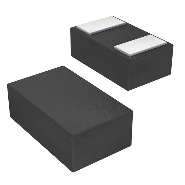
The device is housed in a compact X3DFN2 (0201) surface mount package with body dimensions of 0.62 x 0.32 x 0.3 mm, making it suitable for space-constrained designs. It is Pb-free, halogen free/BFR free, and RoHS compliant. Operating temperature range is -55°C to 150°C.
The working reverse voltage (VRWM) is ±18.5V maximum, bidirectional symmetrical.
The typical clamping voltage is 35V.
The peak pulse current is 1A for an 8/20µs waveform per IEC 61000-4-5.
The typical capacitance is 0.3pF at 1MHz.
It meets IEC 61000-4-2 Level 4: 15kV air discharge and 12kV contact discharge.
It is available in a 2-X3DFN (0.6x0.3) (0201) surface mount package with body size 0.62 x 0.32 x 0.3 mm.
The junction and storage temperature range is -55°C to 150°C.