

| Distributor | Stock | Pricing | MOQ | PKG | Lead Time | Date Code | On Order Quantity | On Order Delivery | |
|---|---|---|---|---|---|---|---|---|---|
|
1,000 pcs
|
1000 pcs | On Request | 1 | On Request | On Request | On Request | On Request | On Request |
| Category | |
| Manufacturer Name | |
| Configuration | |
| Current | |
| Drain to Source Voltage (Vdss) | |
| Gate Charge (Qg) (Max) @ Vgs | |
| Input Capacitance (Ciss) (Max) @ Vds | |
| Lead Style | |
| Mounting Type | |
| Operating Temperature | |
| Rds On (Max) @ Id, Vgs | |
| Storage Temperature | |
| Supplier Device Package | |
| Technology | |
| Termination Style | |
| Vgs(th) (Max) @ Id |
The EPC2110ENGRT is a dual common-source enhancement-mode GaN power transistor from EPC, designed for high-efficiency power conversion applications. Each device integrates two N-channel GaN FETs with a common source configuration, providing a 120V drain-source voltage rating and 3.4A continuous drain current. The typical on-resistance is 80 mΩ, with a maximum of 110 mΩ at 5V gate drive.
This transistor features ultra-low gate charge (0.8 nC typical) and zero reverse recovery charge, enabling high-frequency switching with minimal losses. The operating junction temperature range spans -40°C to 150°C, with a junction-to-case thermal resistance of 3°C/W. The device is well-suited for applications requiring high efficiency and compact size.
Typical applications include ultra-high frequency DC-DC conversion, wireless power transfer, and synchronous rectification. The GaN technology offers superior figure of merit compared to silicon MOSFETs, particularly in hard-switching and resonant topologies.
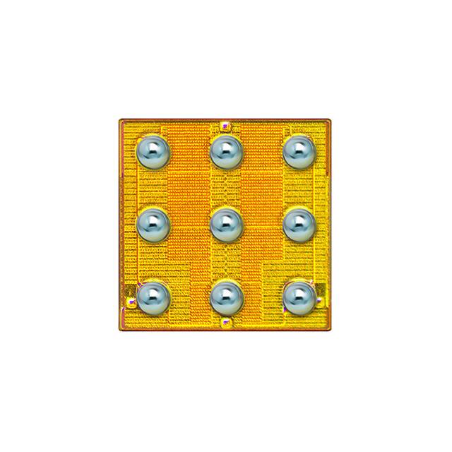
The EPC2110ENGRT is offered in a die form factor with solder bump terminals for surface mount assembly. The die size is 1.35 x 1.35 mm, and the device is RoHS3 compliant with MSL 1 rating.
| Qty | Low | High |
|---|---|---|
| 2,500+ | $0.91 | $0.91 |
Estimated market price range - modelled values for guidance only, not live distributor offers.
The maximum drain-to-source voltage is 120 V.
The device is supplied in a die package with solder bump terminals for surface mount assembly.
The operating junction temperature range is -40°C to 150°C.
Yes, the device is RoHS3 compliant (unverified, low confidence).
The continuous drain current is 3.4 A at 25°C.
The typical on-resistance is 80 mΩ at 5V gate voltage and 4A drain current.
The gate threshold voltage ranges from 0.8V minimum, 1.4V typical, to 2.5V maximum at 0.7 mA drain current.