

| Distributor | Stock | Pricing | MOQ | PKG | Lead Time | Date Code | On Order Quantity | On Order Delivery | |
|---|---|---|---|---|---|---|---|---|---|
|
60 pcs
|
60 pcs | On Request | 1 | On Request | On Request | On Request | On Request | On Request |
| Category | |
| Manufacturer Name | |
| Lead Spacing | |
| Mounting Type | |
| Number of I | |
| Number of LABs | |
| Number of Logic Elements | |
| Operating Temperature | |
| Supplier Device Package | |
| Total RAM Bits | |
| Voltage |
The Intel EP4CGX75DF27C8N is a mid-sized FPGA from the Cyclone IV GX series, designed for logic integration and high-speed applications. It offers 73920 logic elements and 4620 logic array blocks, providing substantial capacity for custom hardware logic programming.
This FPGA includes 4.26 Mbits of embedded RAM and supports 310 input/output pins, making it suitable for complex digital designs. The operating voltage range is between 1.16V and 1.24V, and it operates within a junction temperature range of 0°C to 85°C.
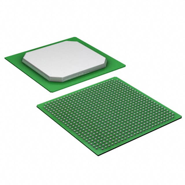
The device is housed in a 672-ball Fine-Pitch Ball Grid Array (FBGA) package, measuring 27x27mm, and is designed for surface mounting. Its architecture is built on the Cyclone IV GX core, featuring internal programmable logic grouped into logic array blocks, along with embedded RAM and configurable I/O.
This FPGA supports flexible hardware logic programming for custom functions, enabling its use in a variety of embedded systems requiring custom digital processing capabilities.
The EP4CGX75DF27C8N FPGA has 73920 logic elements.
The EP4CGX75DF27C8N offers 310 I/O pins.
The EP4CGX75DF27C8N has a total of 4257792 embedded RAM bits.
The operating voltage range for the EP4CGX75DF27C8N is 1.16V to 1.24V.
The operating temperature range for the EP4CGX75DF27C8N is 0°C to 85°C (TJ).
The EP4CGX75DF27C8N is supplied in a 672-BGA package.
The mounting type for the EP4CGX75DF27C8N is Surface Mount.