

| Distributor | Stock | Pricing | MOQ | PKG | Lead Time | Date Code | On Order Quantity | On Order Delivery | |
|---|---|---|---|---|---|---|---|---|---|
|
480 pcs
|
480 pcs | On Request | 1 | On Request | On Request | 17+ | On Request | On Request |
| Category | |
| Manufacturer Name | |
| Lead Spacing | |
| Mounting Type | |
| Number of I | |
| Number of I/O | |
| Number of LABs | |
| Number of LABs/CLBs | |
| Number of Logic Elements | |
| Number of Logic Elements/Cells | |
| Operating Temperature | |
| Supplier Device Package | |
| Total RAM Bits | |
| Voltage |
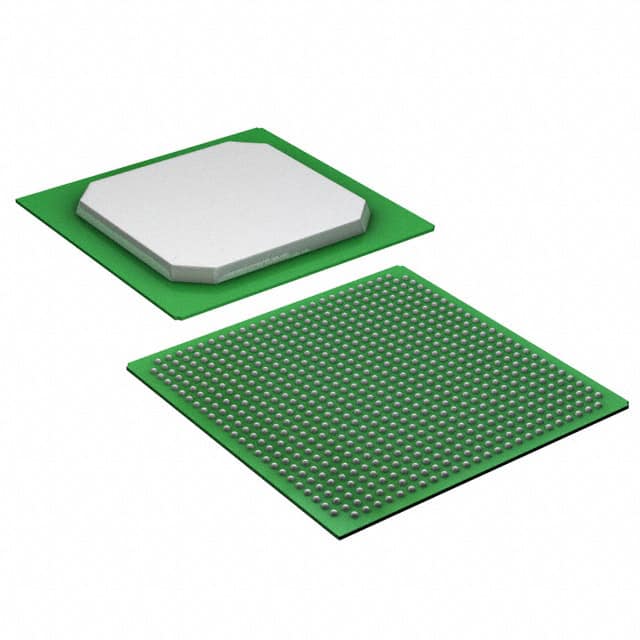
This Intel EP4CGX110DF27C7N is a member of the Cyclone IV GX FPGA family. It features 109,424 logic elements and 6,839 configurable logic blocks (CLBs), providing substantial capacity for complex digital designs. The device includes 5,621,760 total RAM bits for on-chip data buffering and processing.
With 393 user I/O pins, this FPGA offers flexible connectivity for various applications. It operates within a supply voltage range of 1.16V to 1.24V and is designed for a junction operating temperature of 0°C to 85°C. The component is mounted using surface mount technology and comes in a 672-FBGA (27x27 mm) package.
Suitable for applications requiring hardware reconfigurability, such as industrial automation, communication equipment, video/image processing, and embedded computing platforms. Its high logic density and abundant I/Os make it a strong choice for demanding design tasks.
The operating supply voltage is 1.16V to 1.24V.
The EP4CGX110DF27C7N FPGA has 109,424 logic elements.
The EP4CGX110DF27C7N FPGA has 5,621,760 total RAM bits.
The EP4CGX110DF27C7N FPGA has 393 I/O pins.
The operating junction temperature range is 0°C to 85°C.
The EP4CGX110DF27C7N FPGA is supplied in a 672-FBGA (27x27 mm) package.
The EP4CGX110DF27C7N FPGA requires surface mount technology.