

| Distributor | Stock | Pricing | MOQ | PKG | Lead Time | Date Code | On Order Quantity | On Order Delivery | |
|---|---|---|---|---|---|---|---|---|---|
|
3 pcs
|
3 pcs | On Request | 1 | On Request | On Request | On Request | On Request | On Request |
| Category | |
| Manufacturer Name | |
| Lead Spacing | |
| Mounting Type | |
| Number of I | |
| Number of LABs | |
| Number of Logic Elements | |
| Operating Temperature | |
| Supplier Device Package | |
| Supplier Package | |
| Total RAM Bits | |
| Voltage | |
| Voltage Supply |
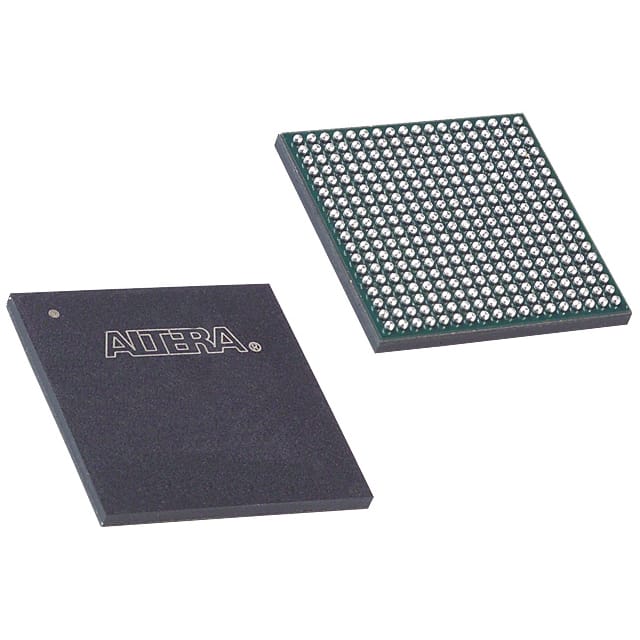
The Intel EP3C25F324C6N is a field programmable gate array (FPGA) designed for embedded applications. It contains 24,624 logic elements and 1,539 logic array blocks, providing substantial programmable logic capacity. The device includes 608,256 RAM bits and 215 input/output pins, making it suitable for complex digital designs.
This FPGA is packaged in a 324-ball BGA (Ball Grid Array) with a 19x19 mm footprint, suitable for surface mounting on printed circuit boards. It operates within a voltage range of 1.15V to 1.25V and supports operating temperatures from 0°C to 85°C. The device is compliant with RoHS standards, although this status is unverified. It is intended for use in embedded systems requiring high logic density and I/O flexibility.
Designed for applications such as digital signal processing, communications, and industrial automation, the EP3C25F324C6N offers a reliable and versatile platform for complex FPGA implementations. Its surface-mount package facilitates integration into compact electronic assemblies.
The EP3C25F324C6N contains 24,624 logic elements.
The device has 215 I/O pins.
It operates within a voltage range of 1.15V to 1.25V.
It is housed in a 324-BGA package.
It operates from 0°C to 85°C.