

| Distributor | Stock | Pricing | MOQ | PKG | Lead Time | Date Code | On Order Quantity | On Order Delivery | |
|---|---|---|---|---|---|---|---|---|---|
|
3,500 pcs
|
3500 pcs | On Request | 1 | On Request | On Request | On Request | On Request | On Request |
| Category | |
| Manufacturer Name | |
| Lead Spacing | |
| Mounting Type | |
| Number of I | |
| Number of I/O | |
| Number of LABs | |
| Number of Logic Elements | |
| Operating Temperature | |
| Supplier Device Package | |
| Supplier Package | |
| Total RAM Bits | |
| Voltage |
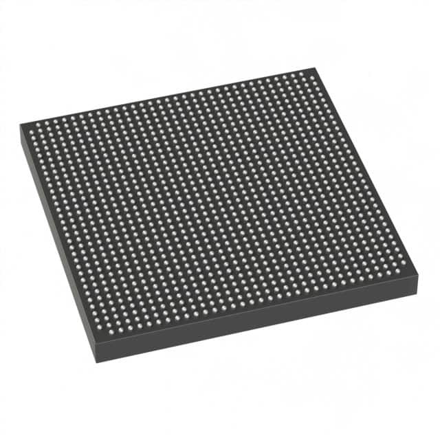
The Intel EP2SGX90EF1152C3N is a Field Programmable Gate Array (FPGA) belonging to the Stratix II GX family. This device offers a substantial logic density with 90,960 logic elements and 4,548 Logic Array Blocks (LABs), complemented by 4,520,448 bits of RAM.
Designed for high-speed applications, it provides 558 I/O pins and operates within a voltage range of 1.15V to 1.25V. The operating temperature range is specified from 0°C to 85°C (TJ).
This FPGA is packaged in an 1152-FBGA (35x35) format and is designed for surface mount applications. Its robust feature set makes it suitable for complex digital designs in telecommunications, networking, and industrial automation.
The Stratix II GX architecture, upon which this device is built, offers a 1.2-V logic array with high performance and flexibility, ideal for applications requiring high-speed backplane interfaces, chip-to-chip communication, and protocol bridging.
The EP2SGX90EF1152C3N FPGA has 90,960 logic elements.
The EP2SGX90EF1152C3N features 558 I/O pins.
The operating voltage range for the EP2SGX90EF1152C3N is 1.15V to 1.25V.
The EP2SGX90EF1152C3N is supplied in a 1152-FBGA (35x35) package.
The EP2SGX90EF1152C3N operates within a temperature range of 0°C to 85°C (TJ).