

| Distributor | Stock | Pricing | MOQ | PKG | Lead Time | Date Code | On Order Quantity | On Order Delivery | |
|---|---|---|---|---|---|---|---|---|---|
|
3 pcs
|
3 pcs | On Request | 1 | On Request | On Request | On Request | On Request | On Request |
| Category | |
| Manufacturer Name | |
| Lead Spacing | |
| Mounting Type | |
| Number of I | |
| Number of LABs | |
| Number of Logic Elements | |
| Operating Temperature | |
| Supplier Device Package | |
| Total RAM Bits | |
| Voltage |
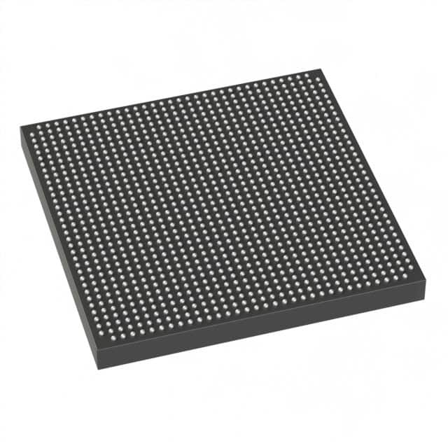
The Intel EP2SGX90EF1152C3 is a Field Programmable Gate Array (FPGA) belonging to the Stratix II GX family. This device offers a substantial 90,960 logic elements and 4,548 Logic Array Blocks (LABs), providing significant processing power for complex digital designs. It includes 4,520,448 total RAM bits for efficient data buffering and operations.
With 558 high-speed I/O pins, the EP2SGX90EF1152C3 is well-suited for parallel data transfer applications. It operates within a voltage range of 1.15V to 1.25V, optimizing power consumption. The device is designed for surface mounting and comes in a 1152-FBGA (35x35) package, supporting an operating temperature range of 0°C to 85°C (TJ).
The Stratix II GX architecture is built for high-performance applications, including high-speed backplane interfaces, chip-to-chip communication, and protocol bridging. These FPGAs combine high-speed serial transceivers with a scalable logic array, making them ideal for demanding telecommunications, data center infrastructure, networking equipment, and aerospace systems.
The EP2SGX90EF1152C3 has 90,960 logic elements.
The EP2SGX90EF1152C3 features 558 I/O pins.
The operating voltage range for the EP2SGX90EF1152C3 is 1.15V to 1.25V.
The EP2SGX90EF1152C3 is supplied in a 1152-FBGA (35x35) package.
The operating temperature for the EP2SGX90EF1152C3 is 0°C to 85°C (TJ).
The EP2SGX90EF1152C3 has a total of 4,520,448 RAM bits.
The EP2SGX90EF1152C3 contains 4,548 Logic Array Blocks (LABs).