

| Distributor | Stock | Pricing | MOQ | PKG | Lead Time | Date Code | On Order Quantity | On Order Delivery | |
|---|---|---|---|---|---|---|---|---|---|
|
2,568 pcs
|
2568 pcs | On Request | 1 | On Request | On Request | On Request | On Request | On Request |
| Category | |
| Manufacturer Name | |
| Lead Spacing | |
| Mounting Type | |
| Number of I | |
| Number of I/O | |
| Number of LABs | |
| Number of Logic Elements | |
| Operating Temperature | |
| Supplier Device Package | |
| Total RAM Bits | |
| Voltage | |
| Voltage Supply |
The Intel EP2S30F672C3N is a Field Programmable Gate Array (FPGA) from the Stratix II family. It features 33880 logic elements and 1694 logic array blocks, providing significant processing capabilities for embedded systems.
This FPGA offers 500 I/O pins, allowing for extensive connectivity in complex designs. The operating voltage range is 1.15V to 1.25V, and it is designed for surface mounting within a 0°C to 85°C operating temperature range.
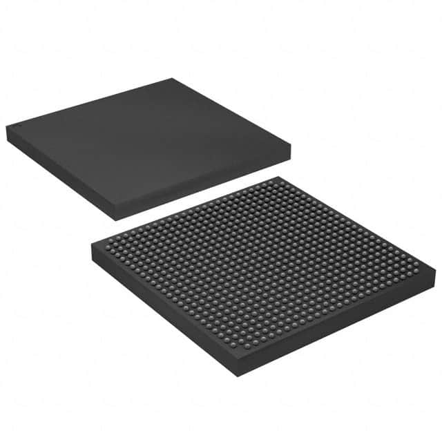
The device comes in a 672-FBGA package, with a 672-BBGA designation for its case. It includes 1,369,728 total RAM bits for data storage and manipulation.
This component is suitable for various digital logic and signal processing applications where high performance and flexibility are required. Its specifications make it a robust choice for advanced embedded system development.
The EP2S30F672C3N FPGA has 33880 logic elements.
The EP2S30F672C3N FPGA has 500 I/O pins.
The operating voltage range for the EP2S30F672C3N FPGA is 1.15V to 1.25V.
The EP2S30F672C3N FPGA is supplied in a 672-FBGA package.
The recommended operating temperature for the EP2S30F672C3N FPGA is 0°C to 85°C (TJ).
The EP2S30F672C3N FPGA can be programmed using Intel Quartus Prime software. It supports JTAG and USB Blaster for programming the device. Ensure that the proper configuration files are created in the Quartus environment for successful programming.