

| Distributor | Stock | Pricing | MOQ | PKG | Lead Time | Date Code | On Order Quantity | On Order Delivery | |
|---|---|---|---|---|---|---|---|---|---|
|
2,336 pcs
|
2336 pcs | On Request | 1 | On Request | On Request | On Request | On Request | On Request |
| Category | |
| Manufacturer Name | |
| Mounting Type | |
| Number of I | |
| Number of LABs | |
| Number of Logic Elements | |
| Operating Temperature | |
| Supplier Device Package | |
| Supplier Package | |
| Total RAM Bits | |
| Voltage |
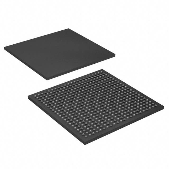
The Intel EP2S30F484C4N is an integrated circuit belonging to the Stratix II family of Field Programmable Gate Arrays (FPGAs). Designed for high-performance applications, this device offers substantial logic capacity with 33,880 logic elements and 1,694 Logic Array Blocks (LABs). It also provides extensive connectivity with 342 I/O pins and robust memory resources, featuring 1,369,728 RAM bits.
This FPGA operates within a flexible supply voltage range of 1.15V to 1.25V and has an operating temperature range of 0°C to 85°C (TJ). It is housed in a 484-pin Fine Ball Grid Array (FBGA) package, measuring 23x23 mm with a 1 mm pitch, and is designed for surface mount applications.
The EP2S30F484C4N is suitable for demanding applications in telecommunications, networking, military and aerospace, and industrial automation. Intel provides development tools such as Quartus II Software to support design, synthesis, and verification.
The operating voltage range is 1.15V to 1.25V.
The device supports 342 I/O pins.
It is housed in a 484-pin Fine Ball Grid Array (FBGA) package.
The operating temperature range is 0°C to 85°C (TJ).
The device features 33,880 logic elements.
It features a total of 1,369,728 RAM bits.