

| Distributor | Stock | Pricing | MOQ | PKG | Lead Time | Date Code | On Order Quantity | On Order Delivery | |
|---|---|---|---|---|---|---|---|---|---|
|
4,000 pcs
|
4000 pcs | On Request | 1 | On Request | On Request | On Request | On Request | On Request |
| Category | |
| Manufacturer Name | |
| Mounting Type | |
| Number of I | |
| Number of I/O | |
| Number of LABs | |
| Number of Logic Elements | |
| Operating Temperature | |
| Operating Voltage | |
| Supplier Device Package | |
| Total RAM Bits | |
| Voltage |
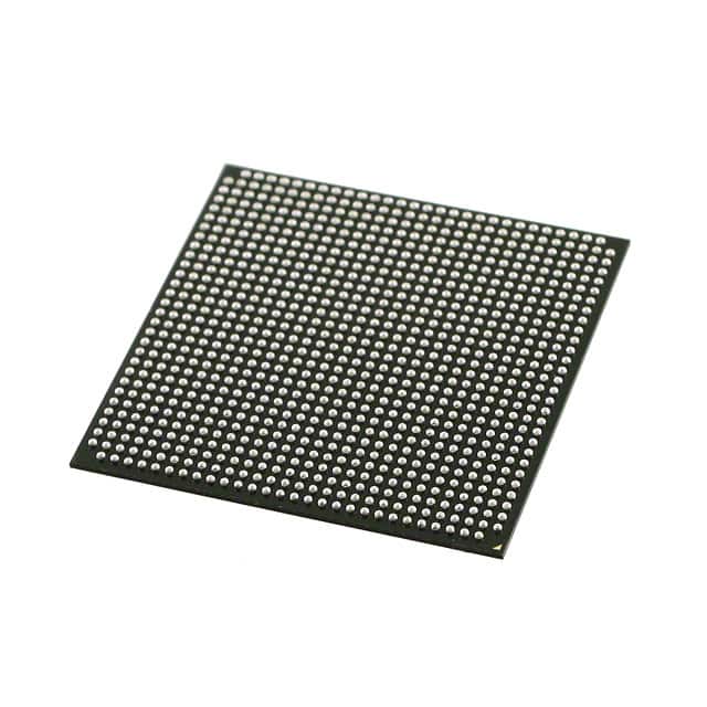
The Intel EP2C70F896I8 is a Field Programmable Gate Array (FPGA) from the Cyclone II family. It features 68416 logic elements organized into 4276 logic array blocks, providing substantial processing capability for complex digital designs.
This FPGA offers 1,152,000 total RAM bits for embedded memory and buffering. It supports 622 general-purpose input/output pins, enabling extensive peripheral interfacing. The device operates within a voltage range of 1.15V to 1.25V and is designed for reliable operation across an industrial temperature range of -40°C to 100°C (junction).
The EP2C70F896I8 is packaged in an 896-BGA (896-FBGA (31x31)) and is designed for surface mounting. Its specifications make it suitable for applications requiring moderate logic density, significant memory, and high I/O count, such as industrial automation, telecommunications, and embedded computing systems.
The operating voltage is 1.15V to 1.25V.
The EP2C70F896I8 FPGA has 68416 logic elements.
The operating temperature range is -40°C to 100°C (TJ).
It is supplied in an 896-BGA package, specifically an 896-FBGA (31x31).
There are 622 I/O pins available.