

| Distributor | Stock | Pricing | MOQ | PKG | Lead Time | Date Code | On Order Quantity | On Order Delivery | |
|---|---|---|---|---|---|---|---|---|---|
|
3 pcs
|
3 pcs | On Request | 1 | On Request | On Request | On Request | On Request | On Request |
| Category | |
| Manufacturer Name | |
| Mounting Type | |
| Number of I | |
| Number of LABs | |
| Number of Logic Elements | |
| Operating Temperature | |
| Supplier Device Package | |
| Total RAM Bits | |
| Voltage |
The Intel EP2C50F484C8N is a Field Programmable Gate Array (FPGA) from the Cyclone II family. This device features 50,528 logic elements and 3,158 logic array blocks (LABs), providing substantial capacity for complex digital designs. It offers 294 input/output (I/O) pins, enabling extensive interfacing capabilities.
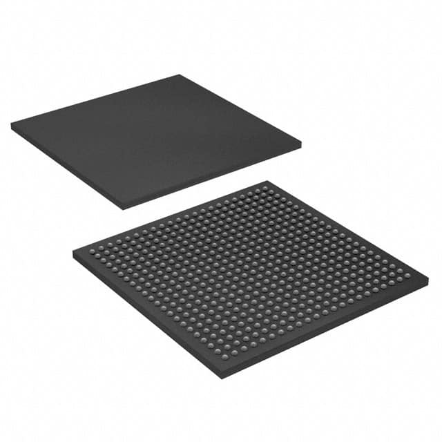
The FPGA operates within a voltage supply range of 1.15V to 1.25V and is designed for operation across a temperature range of 0°C to 85°C (TJ). The component is supplied in a 484-FBGA package, measuring 23x23 mm, and utilizes surface mount technology for integration into printed circuit boards.
With 594,432 total RAM bits, the EP2C50F484C8N is suitable for applications requiring on-chip memory. Its robust feature set makes it a versatile solution for embedded processing and digital signal processing tasks.
The operating temperature range for the Intel EP2C50F484C8N FPGA is 0°C to 85°C (TJ).
The voltage supply range for the EP2C50F484C8N FPGA is 1.15V to 1.25V.
The EP2C50F484C8N FPGA has 50,528 logic elements.
The Intel EP2C50F484C8N comes in a 484-FBGA (23x23) package.
Users commonly encounter configuration failures, incompatibility with toolchains, and power supply issues when using the Intel EP2C50F484C8N FPGA.