

| Distributor | Stock | Pricing | MOQ | PKG | Lead Time | Date Code | On Order Quantity | On Order Delivery | |
|---|---|---|---|---|---|---|---|---|---|
|
3,600 pcs
|
3600 pcs | On Request | 1 | On Request | On Request | On Request | On Request | On Request |
| Category | |
| Manufacturer Name | |
| Frequency | |
| Mounting Type | |
| Number of I | |
| Number of LABs | |
| Number of Logic Elements | |
| Operating Temperature | |
| Package / Case | |
| Supplier Device Package | |
| Total RAM Bits | |
| Voltage |
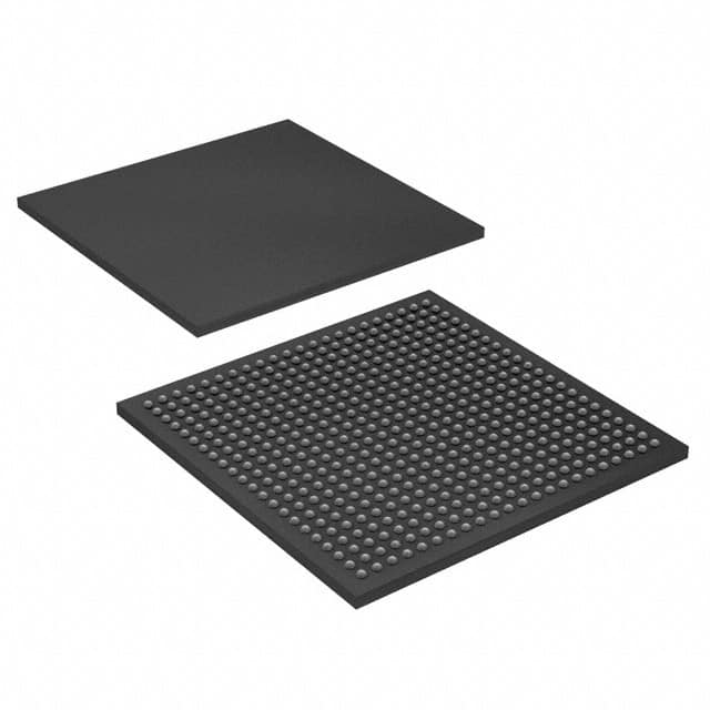
The Intel EP2C35F484C7 is a Field Programmable Gate Array (FPGA) belonging to the Cyclone II family. This integrated circuit offers robust computational capabilities with 33,216 logic elements and 2,076 Logic Array Blocks (LABs). It provides extensive connectivity with 322 I/O pins, making it suitable for complex digital designs.
The device operates within a supply voltage range of 1.15V to 1.25V and has an operating temperature range of 0°C to 85°C (TJ). It features a total of 483,840 RAM bits for ample memory requirements. The EP2C35F484C7 is designed for surface mounting and comes in a 484-FBGA package.
Applications for the EP2C35F484C7 include telecommunications, industrial automation, consumer electronics, and automotive systems. Development is supported by Intel's Quartus II Software and various IP cores.
The operating temperature range is 0°C to 85°C (TJ).
The supply voltage is between 1.15V and 1.25V.
The EP2C35F484C7 features 322 I/O pins.
The EP2C35F484C7 is supplied in a 484-FBGA package.
The EP2C35F484C7 has 33,216 logic elements.
The EP2C35F484C7 has a total of 483,840 RAM bits.