

| Distributor | Stock | Pricing | MOQ | PKG | Lead Time | Date Code | On Order Quantity | On Order Delivery | |
|---|---|---|---|---|---|---|---|---|---|
|
2 pcs
|
2 pcs | On Request | 1 | On Request | On Request | On Request | On Request | On Request |
| Category | |
| Manufacturer Name | |
| Lead Spacing | |
| Mounting Type | |
| Number of I | |
| Number of I/O | |
| Number of LABs | |
| Number of LABs/CLBs | |
| Number of Logic Elements | |
| Number of Logic Elements/Cells | |
| Operating Temperature | |
| Supplier Device Package | |
| Total RAM Bits | |
| Voltage | |
| Voltage Supply |
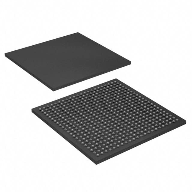
The Intel EP2C20F484C7 is a Field Programmable Gate Array (FPGA) from the Cyclone II family. This device offers 315 input/output (I/O) pins and is built with 18752 logic elements and 1172 logic array blocks (LABs). It includes a total of 239616 RAM bits for on-chip memory.
Designed for embedded processing and DSP solutions, this FPGA operates at a supply voltage between 1.15V and 1.25V. The operating temperature range is from 0°C to 85°C (TJ). The component is housed in a 484-BGA package, with the supplier package specified as 484-FBGA (23x23).
Mounting is achieved via a surface mount type. The EP2C20F484C7 is suitable for applications requiring flexible logic implementation and digital signal processing capabilities within its specified operating parameters.
The Intel EP2C20F484C7 FPGA has 18752 logic elements.
The EP2C20F484C7 offers 315 I/O pins.
The operating voltage range for the EP2C20F484C7 is 1.15V to 1.25V.
The Intel EP2C20F484C7 is supplied in a 484-BGA package, specifically a 484-FBGA (23x23).
The operating temperature for the EP2C20F484C7 is 0°C to 85°C (TJ).
The EP2C20F484C7 has a total of 239616 RAM bits.