

| Distributor | Stock | Pricing | MOQ | PKG | Lead Time | Date Code | On Order Quantity | On Order Delivery | |
|---|---|---|---|---|---|---|---|---|---|
|
466 pcs
|
466 pcs | On Request | 1 | On Request | On Request | On Request | On Request | On Request |
| Category | |
| Manufacturer Name | |
| Mounting Type | |
| Number of I | |
| Number of I/O | |
| Number of LABs | |
| Number of Logic Elements | |
| Number of Logic Elements/Cells | |
| Operating Temperature | |
| Supplier Device Package | |
| Tape & Reel | |
| Total RAM Bits | |
| Voltage |
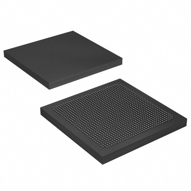
The Intel EP2AGX260FF35C5N is a field programmable gate array (FPGA) designed for high-density digital logic applications. It features 612 I/O pins, enabling extensive connectivity options for various embedded systems. The device includes 12038144 bits of RAM, supporting complex data processing and storage needs. Packaged in a 1152FBGA form factor, it is suitable for surface-mount applications on printed circuit boards.
This FPGA is used in applications requiring high I/O count and substantial internal memory, such as communications, data centers, and advanced embedded systems. Its design allows for flexible programming to meet specific logic requirements, making it a versatile choice for engineers and developers.
The package's 1152FBGA configuration facilitates compact and reliable mounting on circuit boards, supporting high-speed signal integrity and thermal management. The device's electrical specifications include a supply voltage range of approximately 0.87V to 0.93V, ensuring stable operation within typical FPGA power requirements.
The EP2AGX260FF35C5N has 612 I/O pins.
The operating voltage range is approximately 0.87V to 0.93V.
The device is packaged in an 1152FBGA package.
It has 12038144 bits of internal RAM.