

| Distributor | Stock | Pricing | MOQ | PKG | Lead Time | Date Code | On Order Quantity | On Order Delivery | |
|---|---|---|---|---|---|---|---|---|---|
|
2 pcs
|
2 pcs | On Request | 1 | On Request | On Request | On Request | On Request | On Request |
| Category | |
| Manufacturer Name | |
| Mounting Type | |
| Number of Gates | |
| Number of I | |
| Number of LABs | |
| Number of Logic Elements | |
| Operating Temperature | |
| Supplier Device Package | |
| Supply Voltage | |
| Total RAM Bits | |
| Voltage |
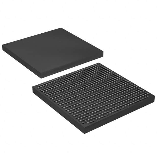
The Intel EP2A15F672C7 is an obsolete Field Programmable Gate Array (FPGA) belonging to the APEX II family. Manufactured using a 0.15-µm process, this device offers a high-density architecture with 1,900,000 system gates and 425,984 RAM bits. It provides 16,640 logic elements and 1,664 Logic Array Blocks (LABs), enabling complex digital designs.
The EP2A15F672C7 supports a wide range of interface standards including True-LVDS, LVPECL, PCML, and HyperTransport, as well as high-speed external memory interfaces like ZBT, QDR, and DDR SRAM/SDRAM. It operates at a low supply voltage of 1.5V and features MultiVolt I/O support for 1.5V, 1.8V, 2.5V, and 3.3V interfaces.
This FPGA is housed in a 672-FBGA package and is designed for surface mount applications. It operates within a temperature range of 0°C to 85°C (TJ). The device is suitable for applications in telecommunications, industrial control, consumer electronics, automotive, and medical devices requiring high-density programmable logic and extensive I/O capabilities.
The EP2A15F672C7 has 16,640 logic elements.
The EP2A15F672C7 features 492 I/O pins.
The operating voltage for the EP2A15F672C7 is between 1.425V and 1.575V.
The EP2A15F672C7 is supplied in a 672-FBGA package.
The EP2A15F672C7 operates within a temperature range of 0°C to 85°C (TJ).
The EP2A15F672C7 supports True-LVDS, LVPECL, PCML, HyperTransport, RapidIO, CSIX, Utopia IV, POS-PHY Level 4, ZBT SRAM, QDR SRAM, DDR SRAM, SDR SDRAM, and DDR SDRAM.