

| Distributor | Stock | Pricing | MOQ | PKG | Lead Time | Date Code | On Order Quantity | On Order Delivery | |
|---|---|---|---|---|---|---|---|---|---|
|
351 pcs
|
351 pcs | On Request | 1 | On Request | On Request | On Request | On Request | On Request |
| Category | |
| Manufacturer Name | |
| Lead Spacing | |
| Mounting Type | |
| Number of I | |
| Number of LABs | |
| Number of Logic Elements | |
| Operating Temperature | |
| Supplier Device Package | |
| Supplier Package | |
| Total RAM Bits | |
| Voltage |
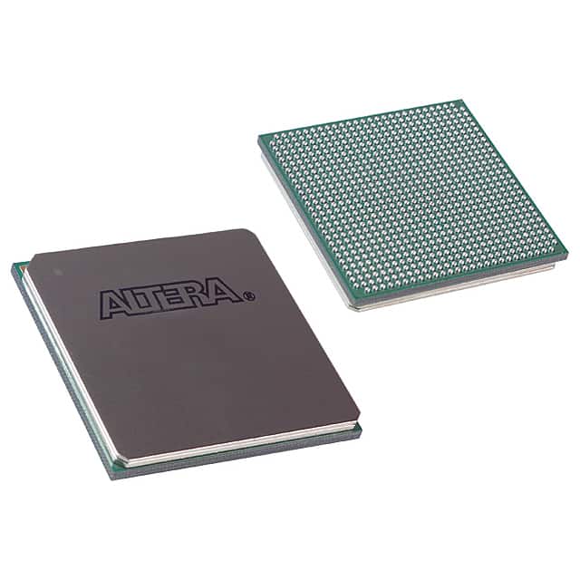
The Intel EP1S40F780C7N is a Field Programmable Gate Array (FPGA) designed for complex digital logic applications. This device features 41,250 logic elements and 4,125 Logic Array Blocks (LABs), providing substantial capacity for custom circuit designs. It offers 615 input/output (I/O) pins, enabling extensive connectivity.
The FPGA includes 3,423,744 total RAM bits for data storage and manipulation. It operates within a voltage range of 1.425V to 1.575V and has an operating temperature range of 0°C to 85°C (TJ). The component is housed in a 780-FBGA (29x29) package, suitable for surface mount applications.
This FPGA is designed for applications requiring high-performance, reconfigurable digital logic. Its specifications make it suitable for various embedded systems and digital signal processing tasks where flexibility and customizability are key requirements.
The operating temperature range is 0°C to 85°C (TJ).
The voltage supply is 1.425V to 1.575V.
The EP1S40F780C7N has 41,250 logic elements.
This FPGA has a total of 3,423,744 RAM bits.
The EP1S40F780C7N features 615 I/O pins.
The EP1S40F780C7N is supplied in a 780-FBGA (29x29) package.