

| Distributor | Stock | Pricing | MOQ | PKG | Lead Time | Date Code | On Order Quantity | On Order Delivery | |
|---|---|---|---|---|---|---|---|---|---|
|
2,476 pcs
|
2476 pcs | On Request | 1 | On Request | On Request | On Request | On Request | On Request |
| Category | |
| Manufacturer Name | |
| Lead Spacing | |
| Mounting Type | |
| Number of Gates | |
| Number of I | |
| Number of LABs | |
| Number of Logic Elements | |
| Operating Temperature | |
| Supplier Device Package | |
| Supplier Package | |
| Total RAM Bits | |
| Voltage |
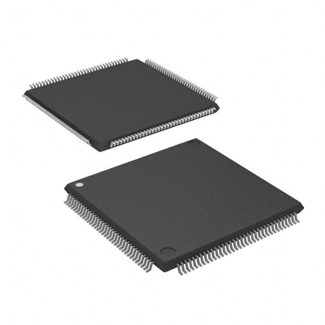
The EP1K10TC144-3N is a field programmable gate array (FPGA) manufactured by Intel. It offers 92 input/output pins and contains 56,000 gates, making it suitable for complex embedded system designs. The device features an internal RAM of 12,288 bits and supports system-on-a-programmable-chip (SOPC) integration with programmable logic devices (PLDs). It is packaged in a 144-pin TQFP surface-mount package measuring 20x20 mm.
Designed for high-density, low-power applications, this FPGA supports multiple voltage levels, including an internal supply voltage of 2.5V. It complies with PCI Local Bus Specification Revision 2.2 for both 3.3V and 5.0V operation, and includes built-in JTAG boundary-scan test circuitry. The device features dual-port capability with up to 16-bit width per embedded array block, enhanced embedded array functions, and low-skew clock distribution trees. It is suitable for use in embedded systems requiring flexible, cost-efficient programmable logic solutions.
The device supports in-circuit reconfigurability via external configuration devices or JTAG, and includes features such as clock management options, global clock and clear signals, and individual tri-state output enables. Its surface-mount 144-TQFP package facilitates integration into compact electronic assemblies.
The FPGA contains 576 logic elements.
It is packaged in a 144-TQFP (20x20) surface mount package.
The device operates at a nominal internal supply voltage of 2.5V.
The FPGA has 92 I/O pins.